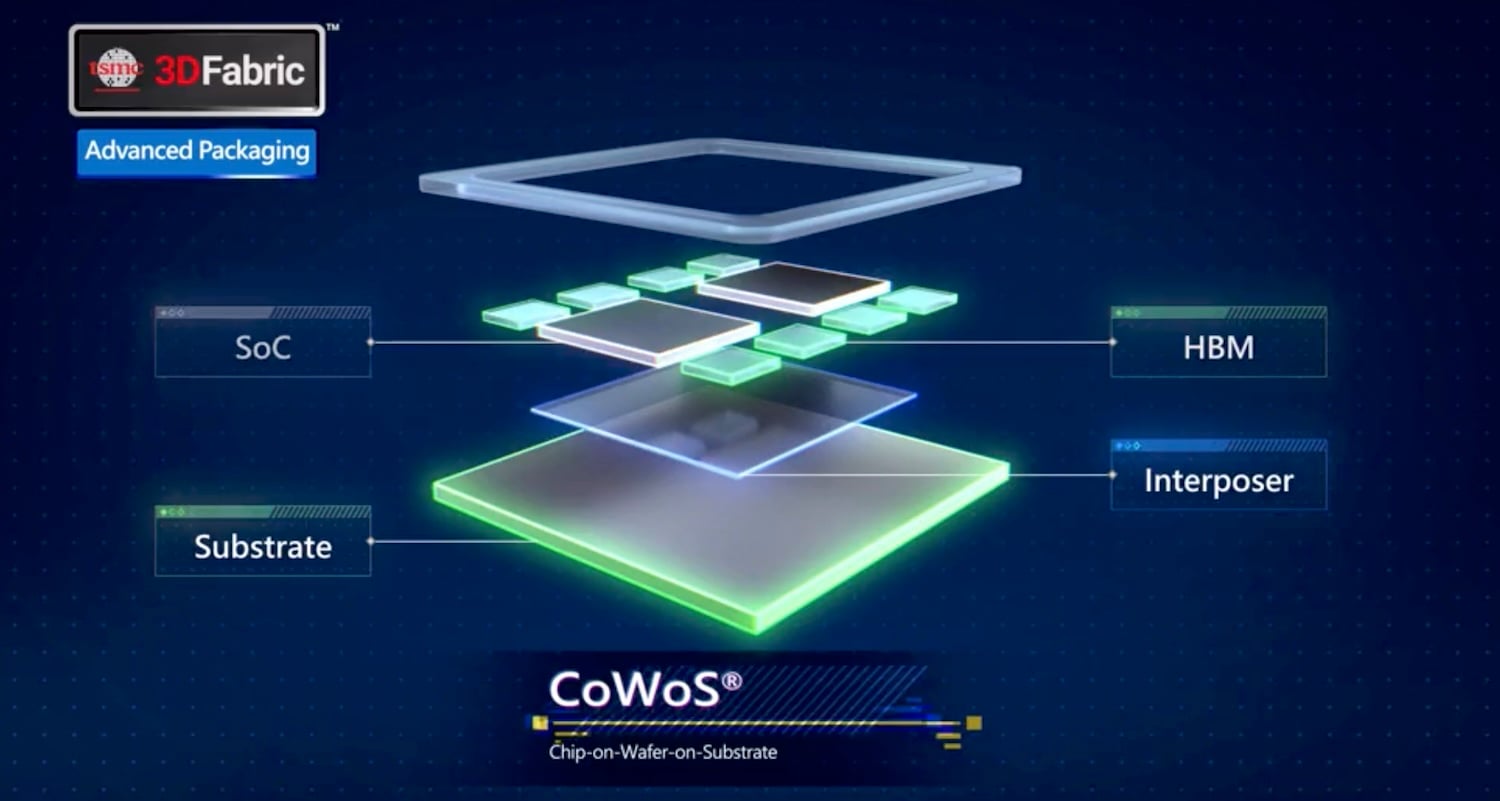
Synopsys has certified its digital and analog EDA flows on TSMC’s A14 process and completed 64G UCIe IP tape-outs on TSMC’s 2nm and 3nm nodes, the two hard milestones in a broader set of joint work the companies announced around TSMC’s Open Innovation Platform ecosystem. The rest of the payload covers agentic AI design flows across Synopsys’ analog, digital, and multi-die tools, integrated voltage regulator co-design on CoWoS packaging, a photonic and electronic co-design flow for TSMC’s COUPE co-packaged optics, and a list of IP tape-outs on N2P that includes PCIe 7.0, HBM4, LPDDR6, and 224G Ethernet.
“As AI systems continue to grow in scale and complexity, customers require proven IP, intelligent design solutions, and advanced packaging methodologies that work together seamlessly,” said Michael Buehler-Garcia, senior vice president at Synopsys. “Our joint innovations with TSMC address the continuum of silicon-to-systems co-design capabilities needed to accelerate development of next-generation AI and high-performance computing systems.”
A14 Certification and Agentic Design Flows #
The A14 certification spans implementation through signoff for both digital and analog flows, which is what a design team needs before it can commit a tape-out to the node. On the analog side, Synopsys and TSMC are working on device routing enablement for A14, which Synopsys describes as a key milestone for advanced analog place-and-route automation. The agentic AI work runs through three tools: Synopsys Custom Compiler accelerates analog migration, Fusion Compiler uses LLM-assisted analysis to boost productivity, and a new agentic chiplet floorplan co-optimization flow in the Synopsys 3DIC Compiler platform automates floorplanning for heterogeneous multi-die designs on TSMC 3DFabric packaging.
Power delivery and optics get their own co-design paths. The 3DIC Compiler platform now lets designers co-design and simulate integrated voltage regulators on TSMC CoWoS in one environment, which Synopsys positions as a way to improve power efficiency and power integrity in multi-die designs as AI packages push power delivery requirements higher. For co-packaged optics, the two companies have an integrated photonic and electronic co-design flow for TSMC’s COUPE technology that spans 3DIC implementation, multiphysics analysis, and optimization, so customers can develop and verify optical interconnect architectures inside a multi-die design.
“Our collaboration with Open Innovation Platform (OIP) ecosystem partners like Synopsys continues to meet the rapidly growing demands of AI and high-performance computing,” said Aveek Sarkar, director of the Ecosystem and Alliance Management Division at TSMC. “By combining certified EDA solutions and silicon-proven IP portfolio from Synopsys with our latest process and packaging innovations, we are enabling customers to push the boundaries of performance, integration, and energy efficiency to shape the future of AI.”
UCIe Silicon and the N2P IP List #
On the die-to-die side, Synopsys demonstrated UCIe-A 32G/40G silicon on a TSMC N3P test chip integrated with a CoWoS-S interposer, and it recently completed 64G UCIe IP tape-outs on both 2nm and 3nm, with embedded DFT for in-system visibility. That’s the same standard that AMD is building into Versal RF for chiplet links, and 64 GT/s is the top data rate in the UCIe 3.0 specification.
On TSMC’s N2P process, Synopsys reports IP enablement and tape-out milestones for PCIe 7.0, HBM4, LPDDR6/5X/5, 224G Ethernet PHY, UCIe, OTP, and Silicon Lifecycle Management process, voltage, and temperature monitoring IP. It has also expanded its silicon-proven Foundation, MIPI, and memory IP for N3P and N2P and is developing IP for TSMC’s compact “C” processes from 6nm through 3nm. The CXL 4.0 IP at 128 GT/s we covered in August sits alongside this portfolio.