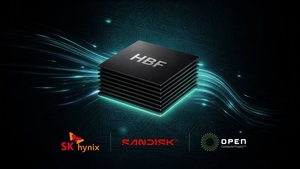
SK hynix and Sandisk have unveiled the first industry standard for high bandwidth flash, seeking to accelerate adoption of a new class of memory designed to bridge the widening performance and capacity gap between high bandwidth memory and solid-state drives.
The specification, released Tuesday and due to be presented when the Future of Memory and Storage 2026 conference opens later in the day in Santa Clara, California, defines HBF products with capacities of up to 512 gigabytes and bandwidth ranging from about 0.4 terabytes to 3 terabytes per second.
HBF combines NAND flash’s high storage capacity with data-transfer speeds closer to those of HBM, which is based on DRAM, placing it between conventional memory and storage in an AI server’s data hierarchy.
The companies are positioning the technology as a way to ease bottlenecks as increasingly complex AI inference workloads require both faster access to data and substantially larger memory pools.
The standard marks the first major outcome of an HBF consortium launched in February, about six months after its formation and a year after SK hynix and Sandisk began working together on standardization. Google and AI chip startup Tenstorrent have also joined the group.
The specification covers products using stacks of eight or 16 NAND dies and divides bandwidth into three performance grades, SK hynix said. It also adopts Universal Chiplet Interconnect Express, or UCIe, allowing HBF devices to connect with different processors, including graphics processing units and central processing units.
The companies disclosed the specifications through the Open Compute Project, making them available as an open industry standard rather than a proprietary format. They also outlined electrical characteristics, packaging and reliability guidelines and software input-output requirements.
The initiative comes as chipmakers and technology companies search for new memory architectures capable of supporting agentic AI systems, which generate large volumes of data and require rapid access to models, databases and intermediate results.
SK hynix said a single type of memory can no longer meet the competing demands for speed, capacity, power efficiency and cost. It is promoting a “tiered memory” architecture that links HBM, HBF, DRAM and storage products and assigns data to each layer according to performance needs.
“HBF will expand the boundary between memory and storage and contribute to new architectures that improve overall system efficiency,” Kim Chun-sung, head of solution development at SK hynix, said.
Kim and Kang Uk-song, head of next-generation product planning, are scheduled to present the tiered-memory strategy in a keynote address at FMS. Executives from SK hynix, Sandisk and Google DeepMind will also hold a panel discussion Thursday on using HBF to overcome the so-called memory wall constraining AI computing.
SK hynix were to separately unveil its tenth-generation, 375-layer 4D NAND technology for the first time at the conference. The company said the product delivers 2.5 times greater performance per watt than the previous generation.
It plans to begin mass production of high-performance, high-capacity enterprise SSDs using the new NAND technology early next year, targeting power-intensive AI data centers.
herim@heraldcorp.com