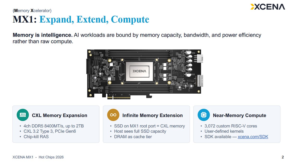
Memory expansion has been attractive for years, and is more relevant than ever because ML models have an insatiable appetite for memory capacity. In response, XCENA has worked with Samsung to create a CXL memory expansion device that can also host SSDs and do compute. The device is called MX1, where MX stands for “Memory Xcelerator”.
On the memory expansion front, the MX1 can host up to 2 TB of DDR5 memory and connects to the host via a PCIe 6/CXL 3.2 x8 interface. The MX1 therefore has 128 GB/s of bandwidth to the host, or 64 GB/s in each direction. XCENA exposes another eight downstream PCIe 6 lanes that can be used to connect SSDs. SSD storage can be exposed as memory, with the MX1’s attached DRAM acting as a cache. The combination of DDR5 slots and downstream PCIe lanes lets the MX1 make a massive amount of memory capacity visible to the host. However, MX1’s most exciting feature is arguably a substantial amount of onboard compute.
MX1’s chip hosts 3072 RISC-V cores, divided into clusters of 32 cores that share L2 caches and a data TLB. Sets of four clusters form a “subsystem”, which acts as the smallest job allocation unit. MX1 has 24 subsystems, letting it run 24 independent jobs at a time. An in-house NoC connects the subsystems to L3 cache and memory. Two Arm Cortex A53 cores handle control functions. The MX1 is fabricated using Samsung’s 4nm process and consumes 40 W, implying that each each RISC-V core draws a bit under 13 mW. The board consumes 90W when accounting for power consumption from 4 DIMMs.
XCENA uses a lot of small cores because they’re targeting data-parallel workloads, where single threaded performance is less important than utilizing high memory bandwidth while maximizing power efficiency. It’s a strategy with parallels to Intel’s Xeon Phi, which similarly used a large number of low-clocked, relatively weak cores to take on highly parallel tasks.
Each RISC-V core uses in-order execution and runs at a pedestrian 1.1 GHz. XCENA’s cache hierarchy is almost GPU-like because it tries to avoid address translation overhead and varies cache sharing wildly at the upper levels. Each core has a 4 KB virtually addressed L1 data cache. Data-side memory accesses don’t go through address translation unless they miss L1D. 128 KB L2 data caches are shared across a cluster, as are TLBs for accelerating address translation. The L2 data cache is virtually indexed and physically tagged (VIPT), much like L1D caches in many conventional CPUs. From the instruction side, sets of four RISC-V cores share a 8 KB instruction cache. XCENA aims to contain kernel hot loops within this instruction cache, while a cluster-level 128 KB L2 instruction cache handles larger instruction footprints.
Instruction fetches operate directly on physical addresses and do not use virtual memory. Instruction accesses therefore don’t need address translation or TLBs. XCENA sets aside predefined device physical addresses for code, and restricts the program counter to those regions. Doing so prevents the RISC-V cores from accidentally jumping to data. XCENA handles process level isolation by isolating jobs at subsystem (128-core) boundaries. Presumably they also divide up the code region to give each subsystem its own code segment, which would prevent one process from accidentally executing another’s code.
MX1’s programming model has parallels to OpenCL or CUDA. One kernel gets invoked many times, and each invocation uses an index to figure out what data it should process. Specifically, mu::getTaskIdx() is analogous to OpenCL’s get_global_id(). This model encourages code sharing across many cores, so sharing L1 instruction caches makes sense. If a loop is small enough, the four cores that share an instruction cache may fetch the same address at the same time, likely letting the instruction cache satisfy multiple fetches with a broadcast read.
On the data side, MX1 uses virtual memory and operates on the same virtual addresses as host code. Host and MX1 code can therefore share pointers, much like with OpenCL’s SVM. XCENA’s software sets up page tables to maintain the same mappings as the host’s. Each RISC-V core has a virtually addressed 4 KB L1 data cache, letting the core avoid address translation on a L1D hit. The cluster-level L2 cache is virtually addressed and physically tagged (VIPT), much like L1D caches on many CPUs. L2 indexing proceeds in parallel with a lookup in the cluster-shared TLB. The TLB has 1024 entries for 64 KB pages, and 8 entries for 1 GB pages. 64 KB pages allow more TLB coverage than typical 4 KB pages, but operating systems tend to use smaller page sizes to reduce overhead when paging to disk, copying pages, or clearing pages. However, XCENA expects the OS to give CXL memory special treatment, and larger page sizes may make sense for a giant block of expansion memory. 64 KB pages also align with typical SSD block sizes. As an aside, using different sets of TLB entries for different page sizes makes sense because it lets the TLB use different indexing schemes for each page size.
Extending RISC-V #
XCENA takes advantage of RISC-V’s extensibility to implement a custom Vector Processing Engine (VPE) at the subsystem level. Each RISC-V core gets a VPE command queue, and can ask the VPE to accelerate a variety of vector operations. Likely, XCENA uses special instructions to enqueue messages into VPE command queues, and expects code to treat it as a giant shared coprocessor. The VPE supports FP32 and FP16, and provides ~3 TFLOPS of dot product throughput across the chip. If the VPEs run at 1.1 GHz like the cores, then each VPE can sustain 128 FLOPS per cycle. Curiously, the VPEs don’t appear to accelerate integer operations. Perhaps XCENA expects code to run integer operations directly on the RISC-V cores. 3072 RISC-V cores at 1.1 GHz would be get roughly 3T integer operations per second if each core completes one operation per cycle. Another curiosity is that XCENA’s API exposes the VPU using built-in functions that return an error code. Code has to explicitly check for error conditions like overflow and invalid accesses, suggesting that VPU instructions don’t raise exceptions.
SSDs as Memory #
MX1 can host SSDs, which are presented to the host as CXL memory. XCENA calls this “Infinite Memory”. MX1 can have SSDs attached in RAID and has matched bandwidth on both its downstream PCIe and upstream PCIe/CXL links, meaning that it can theoretically saturate its bandwidth to the host using SSDs alone. However, SSDs have high latency compared to DRAM. MX1 can mitigate that latency by using its attached DDR5 to cache SSD contents. Caching works with 64 KB pages, with an on-chip 1024 entry map cache. The map cache acts like a TLB, and tracks DRAM pages mapped to SSD-backed addresses. If an access misses in the map cache, it causes a page fault that’s handled by firmware running on the MX1’s RISC-V cores. Firmware handles the cache miss by fetching data from the SSD and updating the mapping. I’m confused because a 1024 entry map cache only covers 64 MB with 64 KB pages, but XCENA’s documentation suggests the cache defaults to 16 GB and has adjustable capacity in 16 MB steps. I’m not sure how that works given the map cache structure.
To further exploit attached DDR5 when using SSD as memory, users can configure a “pinned prefix” where SSD-backed addresses are pinned to DRAM. The pinned prefix region size can be configured in 16 MB steps. Prefixing implies that pinned memory can only cover a contiguous address space, and doesn’t have the flexibility of page-level caching. Therefore, pinned prefix memory is best used to keep a frequently accessed buffer in DRAM. XCENA’s site gives an example with 115.5 GB of pinned memory, out of 231 GB of attached DRAM.
To mitigate SSD latency, the MX1 can also be set up to prefetch from the SSD. Prefetch helps keep the IO path busy, and helps overlap data fetches with compute execution. XCENA hopes to use pinning and prefetch to mitigate a SSD’s low performance compared to DRAM. The MX1 can also run SSDs in RAID to increase bandwidth.
MX1 and LPDDR5X-PIM both place compute close to memory, where they can exploit high internal memory bandwidth that's not accessible over the host interface. MX1 presents a more convincing case than LPDDR5X-PIM because it can act like an accelerator with its own onboard memory. Software doesn’t have to face the tradeoffs and complexity associated with PIM mode switching, and using MX1’s compute won’t block memory accesses from other threads. Host threads and MX1 RISC-V cores could theoretically work on the same buffers, using standard multithreading techniques like locks to ensure ordering.
Working with caches should also be more straightforward than with LPDDR5X-PIM. Type 3 CXL devices (CXL.mem) can use snoops to back-invalidate host cache lines, letting the device make its results visible without resorting to making memory regions uncacheable. Similarly, the CXL.mem device can track read-for-ownership requests from the host and understand when its own compute cores can safely modify data. I’m not sure whether MX1 fully leverages this capability for its RISC-V cores, but Samsung indicates that the device can use CXL memory semantics to share its memory across CPUs and GPUs. Hopefully, that means the device can use snoops to integrate with processor memory subsystems.
As with LPDDR5X-PIM, MX1 doesn’t offer a lot of throughput. For perspective, an Nvidia GeForce GTX 1080 with similar onboard memory bandwidth has 8.8 TFLOPS of FP32 compute, compared to the 3 TFLOPS available from the MX1. But raw throughput isn’t the point. Rather, MX1 offers a way to mitigate some memory expansion downsides. MX1-side compute can avoid the constrained host interface, and avoids the power overhead of traversing the CXL link. A hypothetical accelerator with 8.8 TFLOPS of compute would be limited to just 64 GFLOPS if it had to load one byte per FLOP over CXL. MX1 could exceed 200 GFLOPS in the same scenario, even if it also missed cache.
MX1’s approach to near-memory compute shows promise. CXL memory expanders will often have higher bandwidth to their DRAM pool than what the CXL link can handle. Regular host accesses will leave a large chunk of that bandwidth on the table, which could lead to host-side compute getting memory bandwidth bound if the host can’t serve enough accesses out of its caches. Latency is also a problem because expansion memory will have higher access latency than directly attached memory. A near-memory compute option can mitigate those memory expansion problems without the downsides of attempting the same thing underneath a normal memory controller, as LPDDR5X-PIM does.
I hope to see companies continue to explore memory expanders and near-memory compute in the future. Perhaps in the distant future, this technology can make its way down to consumers. A lot of us have spare DRAM lying around from previous builds, and would be very interested in using it to mitigate the cost of buying new memory. A side of extra compute wouldn’t hurt either.