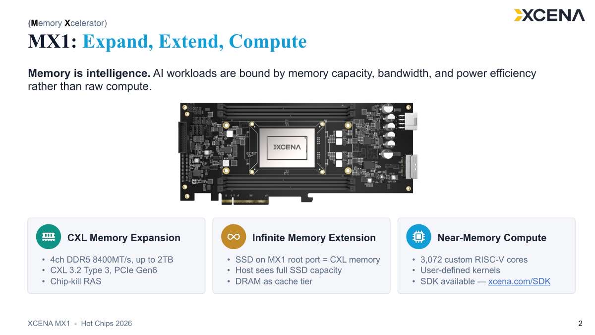
XCENA is presenting its MX1 CXL computational memory device at Hot Chips 2026 in a joint session with Samsung that pairs the device with a rack-scale CXL memory plan. The XCENA MX1 is a Type 3 CXL part that fuses three ideas in one package: CXL memory expansion, SSD-backed storage presented as byte-addressable CXL memory, and near-memory processing across thousands of RISC-V cores. We covered the first generation of MX1 when it appeared as a CXL 3.0 computational memory part, and this session extends that story into rack-scale systems. We are covering this talk live, so please excuse typos.
XCENA MX1 CXL Computational Memory Device at Hot Chips 2026 #
XCENA’s core pitch is that AI workloads stall on memory capacity, bandwidth, and power efficiency before they stall on raw compute. CXL memory expansion spans four DDR5-8400 channels, reaching up to 2TB. Then there is an SSD on the MX1 root port exposed as CXL memory that the host sees in full. Finally, there is near-memory compute across 3,072 custom RISC-V cores. This is so cool.
XCENA built MX1 on Samsung Foundry’s 4nm process and organized the die into 24 subsystems, each composed of four clusters of 32 memory units, for a total of 3,072 MUs. XCENA describes the subsystem as the unit of host job allocation, with each subsystem able to run an independent job and share a 128MB L3 cache.
XCENA chose many simple in-order RISC-V cores over fewer large cores because the target workloads are bandwidth-bound and power-sensitive, and the smaller cores let the company fit 3,072 of them on the die while keeping energy per byte low. An open ISA also provides a mature toolchain and room for custom instructions for data-parallel work, such as in-memory analytics, RAG retrieval, and memory compression.
A Vector Processing Engine adds a vector path on top of the scalar MUs. XCENA delivers roughly 3 TFLOPS of peak dot-product throughput per MX1 SoC, with operations such as element-wise arithmetic, reductions, CRC32, and vector-scalar work, and per-MU command queues aimed at RAG vector search and KV cache scoring.
Locality matters inside the chip. Each cluster shares an 8KB L1 instruction cache among four MUs and a 256KB L2 data cache among its 32 MUs, while a 128MB shared LLC ties the clusters together. Instructions use physical addresses while data uses host virtual addresses, with translation shared at the cluster.
One of the more important software decisions is whether to use a single virtual address space shared by the host and the MUs. Host and device see the same pointers, so pointer-rich structures traverse safely, and existing malloc-based code can move to CXL memory with minimal change, while a CXL-aware allocator keeps per-tenant page tables that isolate one app’s kernels from another’s memory.
On the software side, XCENA ships a MapReduce-style runtime called PXL (the Parallel Xceleration Library). PXL walks an application from device context through kernel definition in C/C++ or Rust, jobs that allocate one or more subsystems, and a map API that splits work across MU cores with allocation and sync handled automatically.
XCENA reports throughput up to 4.7x versus host-over-CXL and 2x versus local DRAM, at roughly a quarter of host power, resulting in efficiency gains of up to 18.7x versus CXL and 6.2x versus DRAM. XCENA ran the comparison on an Intel Xeon 6767P reference, excluding idle power.
Beyond DRAM, MX1 presents SSD capacity as byte-addressable CXL memory via what XCENA calls Infinite Memory, using a DRAM-plus-NAND hybrid in which DRAM caches SSD pages. This SSD is split into 64KB pages, tracked by a 1024-entry map cache TLB. Misses are filled by firmware running on the MU cores. I actually asked XCENA at FMS 2026 about this on the show floor. It is basically a memory tiering solution we have seen a few times over the years, with XCENA’s spin on it. If you are wondering, this is probably a good point in the presentation to bemoan the death of Optane.
Infinite Memory ties directly into the KV cache story. With a pinned prefix that stays resident, XCENA shows query TTFT tracking DRAM at a modest 1.13x, while dropping the pin raises that to 1.57x and a raw SSD baseline to 1.86x. A lookahead prefetch that exploits device underutilization delivers nearly DRAM-resident performance. That test runs Llama-3.1-8B with vLLM, LMCache, and an NVIDIA RTX 6000 Pro. This is a really neat use case to me.
This second half of the session shifts to Samsung’s processing-near-memory research using MX1. Samsung’s analysis centers on using the large DRAM bandwidth behind the CXL interconnect by computing in place and moving only reduced data, with the figure contrasting DDR5 bandwidth at 268.8GB/s against a 64GB/s PCIe Gen6 x8 host link. Maybe the Gen6 x8 link gives away the timing of this since we are just starting to see Gen6 server CPUs launch. Samsung just said on stage that CXL is being adopted by all the major hyperscalers for things like databases and AI/ KV cache.
Samsung and XCENA sketch a rack-scale CXL computational memory system in which GPU servers share memory through CXL memory semantics. This reference appliance pairs a Liqid CXL switch with GPU servers using 96GB NVIDIA RTX Pro 6000 Blackwell parts and targets 20TB of memory capacity at 2.7TB/s of bandwidth.
Samsung brings the NDC API, a near-data-computing library it describes as vendor-agnostic and open-sourced through OCP FTI DCC. Samsung routes PyTorch integration through OpenXLA and PrivateUse1, so an AI framework can reach the XCENA PXL library without code changes.
Samsung’s first AI use case is RAG vector search on CXL-PNM using IVF Flat indexing from FAISS, with the L2 kNN distance computation offloaded because it is memory-bandwidth-bound. Samsung reports 10 PNM devices delivering 64x higher queries per second than a host CPU with a CXL memory pool, and 65x better query-per-energy, built on a 512M-vector FAISS index drawn from Laion 5B.
This second use case is LLM decoding with GPU-plus-PNM hybrid attention. Hybrid attention keeps hit pages on the GPU and pushes miss pages to the PNM device, which returns only the computed attention result instead of shipping the KV pages back. Here, the decode timeline compares GPU-only attention, which loads the KV cache from CXL, with the hybrid path that offloads the missed-attention work.
Samsung’s results on the hybrid decode path are the headline numbers. At 100K context, the PNM pool raises throughput by 3.35x and token-per-energy by 3.84x, shown as 17.7 versus 5.50 tokens per second and 4.31 versus 1.12 tokens per kilojoule. For this run, Samsung used LLaMA-3.1-70B INT8 across two servers, each with five MX1 devices and NVIDIA RTX Pro 6000 Blackwell GPUs.
Taken together, XCENA and Samsung are positioning MX1 as real silicon at the heart of the computational memory wave, pairing the device, its PXL runtime, and Infinite Memory with a rack-scale Samsung pooling story.
Final Words #
XCENA’s session makes a concrete case that the bottleneck for AI and analytics is memory, and that the fix can reside in a CXL device rather than in a larger host processor or a faster GPU. This combination of near-memory RISC-V compute, SSD-backed byte-addressable memory, and Samsung’s rack-scale pooling points to a memory tier that scales capacity and compute together. It will be interesting to see how this works, but I also think that SSD tiering is really interesting.