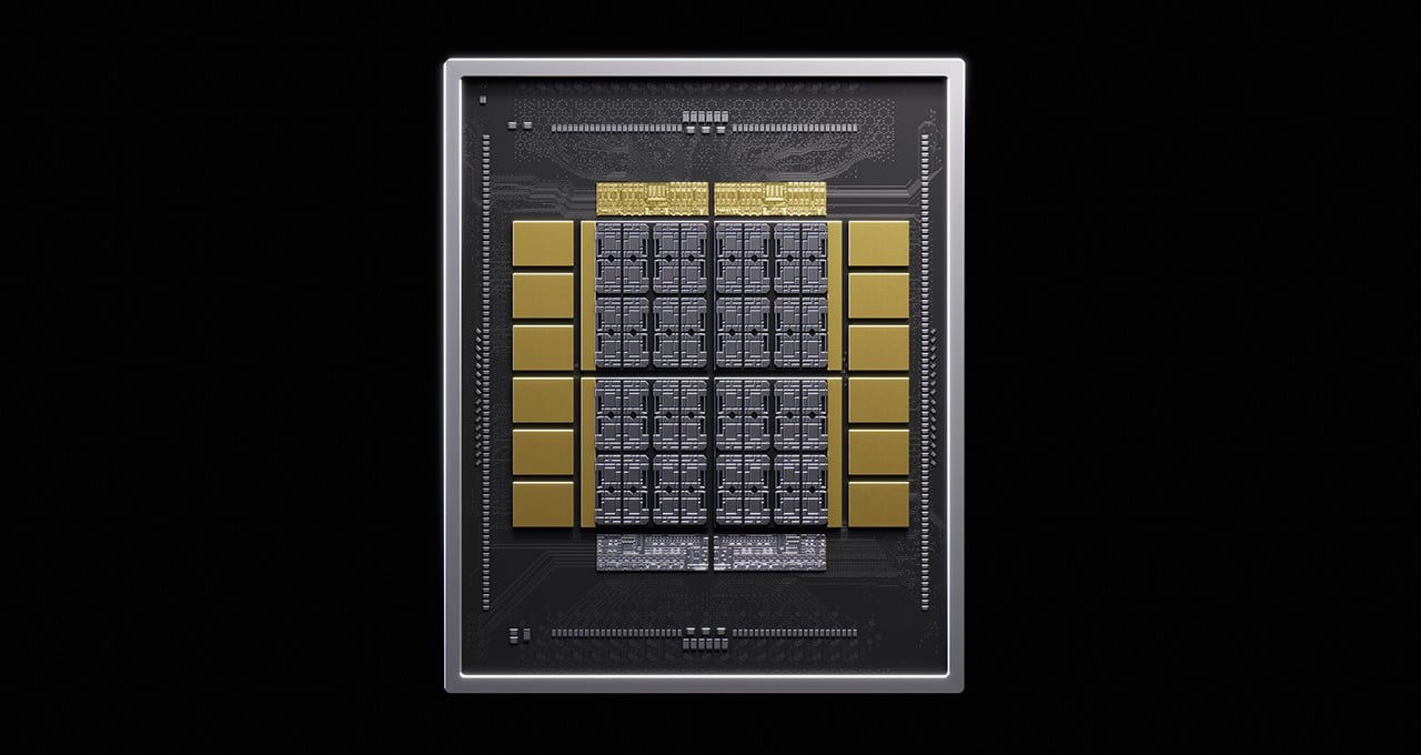
Hyperscalers and AI-focused infrastructure operators are increasingly developing proprietary AI accelerators and XPUs to keep pace with large language models and complex reasoning workloads. To address the physical, memory, and networking challenges of deploying proprietary silicon at scale, NVIDIA has detailed its NVLink Fusion interconnect and NVHBM custom base-die memory architecture. The unified portfolio is designed to bridge custom silicon with NVIDIA’s existing scale-up networking and MGX rack-scale platforms.
The first taker is Amazon’s Annapurna Labs, whose NVHBM plans surfaced alongside the 2 million GPU expansion of the AWS partnership; this announcement supplies the architecture behind that tie-up and names Trainium4 as the first Trainium generation with NVLink Fusion support. NVIDIA is also establishing a standard NVHBM implementation available from multiple memory providers, which it says reduces the engineering effort of integrating and qualifying memory across suppliers. “NVHBM represents a new architectural approach to advancing high-bandwidth memory performance and efficiency,” said Nafea Bshara, vice president of Annapurna Labs at Amazon. “We look forward to this technology collaboration to benefit future AWS infrastructure designs.”
Deploying custom XPUs across high-density data centers requires balancing compute logic, power distribution, thermal overhead, and high-bandwidth memory. Integrating and qualifying leading-edge memory stacks often creates significant packaging and development bottlenecks. Through NVLink Fusion and NVHBM, designers can leverage pre-validated base dies and interface IP, reducing integration complexity and accelerating time-to-market.
Memory Bandwidth and Latency Optimization #
Modern AI workloads, particularly large-model inference and agentic pipelines, place heavy demands on memory throughput for reading model weights, activations, and key-value (KV) cache entries. NVHBM provides a custom base die developed in coordination with memory manufacturers, delivering up to 30 percent higher memory bandwidth per stack compared to the standard JEDEC HBM4E specification.
| Feature | NVHBM benefit | | Bandwidth | Up to 30% more memory bandwidth compared with standard HBM4e | | Area | More efficient interface connections allow up to 25% more compute die area for additional XPU capabilities | | Power | Up to 15% lower HBM power usage compared with standard HBM4e adds up to savings across thousands of XPUs |
Table 1. NVHBM brings three main platform-level advantages to AI accelerator programs: higher memory bandwidth, more package and silicon area, and lower HBM power usage
This bandwidth uplift minimizes compute engine starvation during memory-bound phases of execution. By accelerating data transfers between the HBM stacks and onboard compute logic, accelerators can sustain higher utilization and improve per-user token generation rates during dense inference workloads.
Die Area Reallocation and PHY Optimization #
Silicon real estate on modern accelerator packages is strictly bounded, requiring designers to balance space between compute ALUs, matrix engines, on-chip SRAM, and peripheral interfaces. Standard HBM architectures require wide physical interfaces that consume substantial layout area.
NVHBM addresses this by moving the memory controller directly into the 3D HBM stack and utilizing a custom physical layer (PHY). This approach yields up to a 67 percent reduction in PHY and peripheral support area compared to standard HBM4E implementations, while simplifying interposer trace routing to reclaim up to 80 percent more usable silicon across the layout. The narrower memory interface frees up package real estate, allowing designers to expand the central AI compute die by up to 30 percent to add more matrix cores, vector units, or cache hierarchy within a fixed physical envelope.
Power Efficiency and Facility-Scale Headroom #
Power distribution remains one of the tightest constraints in hyperscale data center operations, directly impacting accelerator thermal design and cooling requirements. NVHBM reduces HBM power consumption by 15 percent compared to standard HBM4E.
At the silicon level, reduced memory power lowers thermal pressure, providing additional electrical headroom to drive compute cores at higher sustained frequencies. At facility scale, these power savings multiply significantly. Across a theoretical 1-gigawatt data center deploying 2,000-watt XPUs, the reduced memory power profile can free up enough thermal and electrical capacity to support up to 15,000 additional XPUs.
Rack-Scale Integration via NVLink Fusion #
While NVHBM optimizes performance at the individual-package level, NVLink Fusion serves as the system-level bridge. Utilizing dedicated NVLink Fusion chiplets, custom XPUs can attach directly to the sixth-generation NVLink scale-up fabric, uniting all accelerators within a rack into a single coherent memory and compute domain. This scale-up fabric is critical for advanced parallelization schemes such as expert parallelism (EP) and WideEP, in which distributed mixture-of-experts models require low-latency synchronization of activations and hidden states across multiple physical devices. Custom processors can also link to host CPUs via NVLink-C2C.
By integrating semi-custom silicon into the broader NVIDIA hardware and software ecosystem, NVLink Fusion enables operators to deploy heterogeneous environments that mix custom XPUs with standard NVIDIA GPUs under a standardized MGX rack architecture, simplifying operations and workload provisioning.