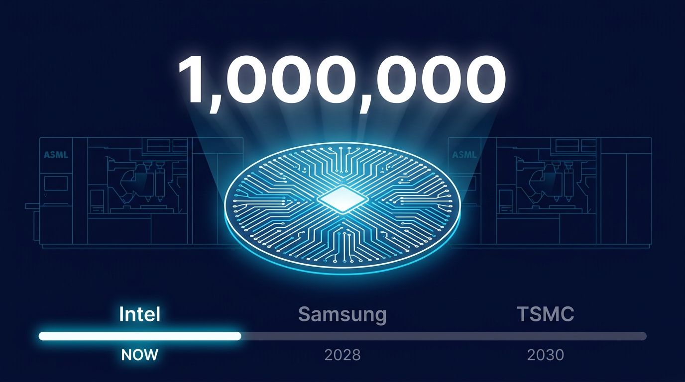
Intel and ASML announced Monday that Intel has processed more than one million wafers on High-NA EUV equipment — a total that exceeds every other chipmaker on earth combined. While September 8 headlines belong to Mistral’s €3 billion raise and GPT-6 Astra’s AGI claims, this number deserves a harder look. TSMC won’t deploy High-NA EUV until 2030. Samsung until 2028. Intel is doing it now, in commercial production, on Panther Lake chips already shipping to customers.
What High-NA EUV Actually Does #
Extreme ultraviolet lithography has been the semiconductor industry’s workhorse for five-nanometer-class chips and below. High-NA EUV is its successor. ASML’s Twinscan EXE:5200B raises the optical system’s numerical aperture from 0.33 to 0.55 — a lens precision upgrade that lets the machine print features at 8nm resolution instead of 13nm. In practical terms: 1.7 times smaller transistors, 2.9 times higher transistor density, achieved with a single exposure rather than the multi-step patterning workaround chipmakers use today. Each machine costs roughly $400 million, twice what a conventional EUV tool runs, and fewer than a dozen exist worldwide.
The Competitive Gap Nobody Is Talking About #
Here is where the milestone gets interesting. Intel has processed more High-NA EUV wafers than Samsung, TSMC, SK Hynix, and every research institution combined. That is not a forecast — it is the cumulative count reported jointly by Intel and ASML on September 8. The competition’s timeline makes the gap concrete:
- Intel: High-NA EUV in commercial production, Panther Lake shipping
- Samsung: Targeting High-NA EUV adoption for DRAM in 2028
- TSMC: Planning to add High-NA EUV layers to logic production starting 2030
Both Samsung and TSMC committed this week to eventually purchasing ASML’s next-generation tools — a meaningful step forward. But commitment and production are different things. Intel is running the machines today.
What This Means for Panther Lake #
Intel’s Core Ultra Series 3 processors, code-named Panther Lake, are the first commercial chips to use High-NA EUV on select manufacturing layers. The critical word is “select” — Intel has not migrated the entire Intel 18A process to High-NA. Specific critical layers run on the EXE systems; the rest use conventional EUV. Yields on those High-NA layers match what Intel achieves on its established NXE platform. Product is shipping.
Panther Lake pairs CPU and GPU cores with a dedicated neural processing unit built for on-device AI inference. The transistor density High-NA EUV enables is what makes a capable NPU possible without ballooning the die area. For developers building local AI applications — on-device inference, privacy-first pipelines, latency-sensitive workloads — this is the silicon foundation those use cases are betting on.
What the Milestone Does Not Prove #
Intel and ASML did not disclose how the one million wafer figure breaks down between equipment qualification runs, process development, and production wafers. That matters. A milestone built heavily on test wafers tells a different story than one driven by customer demand. Intel has not disclosed external customer revenue from 18A — because there isn’t much yet. The foundry business needs Apple, Nvidia, or a hyperscaler to stake a flagship chip on Intel 18A before the comeback narrative becomes a business story rather than a manufacturing story. Reports cite inbound interest from Nvidia, AMD, Apple, Google, and OpenAI on 18A-P and 14A — but interest is not a purchase order.
The 12-Inch Photomask Signal #
The longer-term development worth watching is the coordinated industry push toward 12-inch photomasks. Current High-NA EUV systems use a 6-inch mask format. Intel, ASML, TSMC, and Samsung are co-developing a 12-inch format that could raise High-NA system throughput by up to 40%. A pilot line is planned for 2031, with full production readiness targeted for 2033. That timeline matters because it is when High-NA EUV’s cost per wafer starts becoming competitive at scale. Intel’s head start on 1 million wafers translates directly into process learning that feeds that roadmap.
The Honest Assessment #
Intel’s foundry narrative has been “almost there” for years. The High-NA EUV milestone is different because it is measurable. One million wafers is not a slide deck. It is yield data, defect maps, overlay measurements, and tooling uptime baked into Panther Lake processors in customers’ hands. Intel is 2-4 years ahead of Samsung and TSMC on this specific technology. Whether that lead converts to external foundry revenue — the only metric that validates the strategy — is still an open question. But dismissing the 1 million wafer number as hype would be the same mistake Wall Street made writing off Intel’s 18A progress two years ago. The machines are running. The chips are shipping.