The sub-1nm breakthrough packs nearly double the transistor density of IBM's previous 2nm chip and could reshape the AI and cloud computing hardware landscape
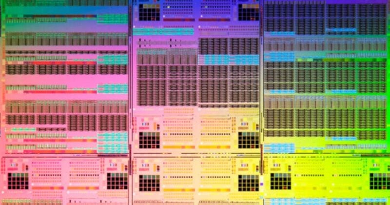
IBM just squeezed roughly 100 billion transistors onto a chip the size of a fingernail. That’s not a typo, and it’s not a theoretical exercise. On June 25, the company unveiled the world’s first 0.7-nanometer chip technology, crossing the sub-1nm threshold that many in the semiconductor world thought was still years away.
To put the scale in perspective: a nanometer is one billionth of a meter. IBM’s new chip operates at 7 angstroms, which is 0.7nm. The technology uses what IBM calls a “nanostack” 3D transistor architecture, a design that stacks components vertically rather than just spreading them across a flat surface.
What the numbers actually mean #
IBM’s previous milestone was its 2nm chip technology, introduced back in 2021. The new 0.7nm design nearly doubles the transistor density of that already cutting-edge predecessor.
IBM says the new architecture could deliver up to 50% better performance compared to current 2nm chips. Alternatively, for applications where power consumption matters more than raw speed, the design could achieve 70% greater energy efficiency.
The company also reported a 40% improvement in SRAM scaling, a key metric for on-chip memory density. These results, along with functional CMOS inverters built using the new process, were presented at VLSI 2026.
The road from lab to factory floor #
For the 0.7nm technology, IBM has lined up manufacturing partners including Lam Research, ASML, TEL, and SCREEN. The technology relies on High-NA extreme ultraviolet lithography, a next-generation chipmaking process that only ASML produces equipment for. IBM has targeted the earliest production within five years, putting potential commercial chips around 2031.
What this means for investors and the broader market #
The AI training and inference market is currently constrained by chip performance and power consumption. A 70% improvement in energy efficiency at the chip level, if it translates to production silicon, would fundamentally change the economics of running large language models and other AI workloads.
For IBM specifically, this announcement reinforces the company’s position as a semiconductor research leader. IBM’s business model in this space relies on licensing its technology and partnering with fabrication companies. The partnership with Lam Research, ASML, TEL, and SCREEN deserves attention from investors watching the semiconductor equipment sector. If 0.7nm technology follows the typical adoption curve, demand for High-NA EUV lithography equipment and related manufacturing tools will climb considerably as production timelines approach.
Disclosure: This article was edited by Editorial Team. For more information on how we create and review content, see our