A breakthrough in 3D silicon stacking could reshape the semiconductor landscape and accelerate AI hardware development
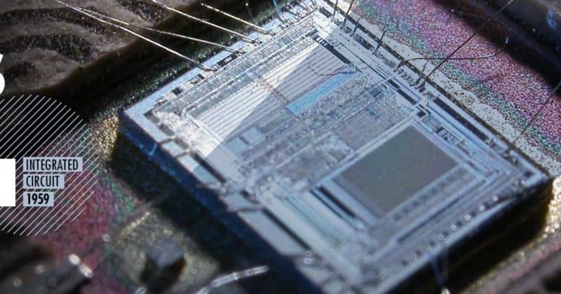
Researchers at the University of Illinois Grainger College of Engineering, working alongside IBM and other chip giants, have published a new method for vertically stacking transistor layers using ultrathin silicon nanomembranes. The results, published in Nature on May 30, 2026, show device yields of 98-100%, a number that makes the technique commercially viable rather than just academically interesting.
How vertical stacking changes the game #
Traditional attempts at 3D chip integration have been hamstrung by heat. Previous methods required temperatures around 400 degrees Celsius, which tended to damage the lower layers of circuitry already in place.
The Illinois team solved this by using junctionless transistors built on silicon nanomembranes just 10 nanometers thick. Their process works at temperatures of 200 degrees Celsius or below, which keeps existing layers intact.
The researchers demonstrated three stacked layers, each containing 625 transistors, achieving current densities on par with conventional bulk silicon devices.
IBM is one of several major industry partners involved, alongside Intel and TSMC, through the Center for Advanced Semiconductor Chips with Accelerated Performance.
IBM’s semiconductor track record #
Back in 2021, IBM unveiled a prototype chip built on 2 nm process technology, packing roughly 50 billion transistors onto a single chip. At the time, it was the most advanced chip architecture ever announced.
What this means for investors and the AI hardware race #
Investors should pay attention to how quickly this technology moves from lab demonstration to pilot production. A three-layer stack of 625 transistors each is a proof of concept. The 98-100% yield numbers are encouraging on that front, since yield is typically the metric that kills promising chip technologies before they reach the factory floor.
Disclosure: This article was edited by Editorial Team. For more information on how we create and review content, see our