In this advanced deep dive, I will discuss the challenges of scaling HBM performance.
Part 1: A High-Level History of HBM: From Commodity to AI’s Most Critical Component
- JEDEC Standards
- From Commodity to AI’s Most Critical Component
- Why is HBM needed for AI?
- Alternative Memories to HBM
Part 2: System Breakdown of HBM
- DRAM Principle of Operation
- Core Die Features
- Base Die Features
- Example Architecture: Samsung HBM4 Architecture - ISSCC 2026
- Where Major Memory Makers Differentiate (SK Hynix, Samsung, Micron)
🔒Part 3: Major Scaling Limits and Conventional Solutions
- 🔒Thermal Gradient in the Stackup
- 🔒Reliability, Availability, Serviceability (RAS) Challenges from Stacking
- 🔒Area Inefficiency from TSVs
- 🔒Signal Integrity Physics Limits from “Wide and Slow”
🔒Part 4: Emerging Trends to Scale Performance
- 🔒Hybrid Bonding
- 🔒Switching to Logic Node for the Base Die and Off Features from XPU
- 🔒Direct Memory Extension from Base Die
- 🔒3D Integration
The current HBM architecture is running into several scaling challenges from thermal performance, interconnect shoreline limits, and manufacturing yield.
In my opinion, I think the #1 problem with HBM is thermal gradients in the stack. The temperature can vary greatly at different layers in the stack, requiring sophisticated sensors and circuits to compensate for thermal mismatches.
I previously wrote a deep dive on the signal integrity challenges of scaling wide-and-slow I/O HBM architectures. I also wrote a companion piece covering the #2 most important memory that operates alongside HBM, SRAM, and what fundamentally limits its scaling:
High bandwidth memory (HBM) is arguably the single most important component in AI accelerators because its capacity is large enough to store a lot of data involved in AI computation, including model weights, gradients, optimizer states, and activations.
High data bandwidth is essential because most AI compute is strained by data movement between memory and compute, not the raw horsepower of the compute itself. Unfortunately, memory bandwidth has not kept pace with compute scaling, leading to the well-known von Neumann bottleneck.
JEDEC Standards
For much of its history, the memory industry has been very conservative in order to endure cycles of boom and bust. Memory products have historically operated under highly commoditized volume markets driven by strict JEDEC (Joint Electron Device Engineering Council) standards. This standardization is necessary to make memory chips functionally interchangeable across vendors; any electronics manufacturer can purchase a standard DRAM chip from any memory vendor that can plug into any memory controller without customized PHY or custom protocol bridges. Note that JEDEC standardization only applies to the external pin interfaces; the internal die implementation is up to the manufacturer. JEDEC standardization made competition between memory manufacturers almost entirely based on pure economic merits, including price-per-bit and manufacturing yield. Unlike GPUs and CPUs with proprietary ISAs, memory makers have historically struggled to differentiate themselves on system functionality.
DRAM has been used as the primary memory source for GPUs due to its high capacity and high BW for highly parallelized computations. Major categories of DRAM include:
- DDR (Double Data Rate) - Optimized for system main memory. Modularity, capacity, and multiple channel flexibility are prioritized.
- LPDDR (Low-Power DDR) - Optimized for power-constrained mobile and edge devices with features such as power gating states and lower operating voltages.
- GDDR (Graphics DDR) - Optimized for high-throughput graphics, gaming consoles, and edge AI hardware with extremely high pin clock frequencies over a narrow bus (~ 32 bits / channel) routed through standard multi-layer PCBs.
GDDR is generally considered the historical predecessor to HBM. GDDR is often referred to as “fast and narrow” and historically placed far away from the GPU (approximately 30 - 100mm).
From Commodity to AI’s Most Important Component
In 2010, GDDR hit severe power and pin-count scaling walls for GPUs. To scale memory performance, either more GDDRs needed to be added or per-pin data rates needed to be pushed higher. Both options were highly undesirable because scaling the number of GDDR blew past physical shoreline limits and real estate of standard chip packages. Higher frequencies caused signal integrity to degrade over long interconnect lengths. Power consumption also increased with CV^2*f.
To overcome these challenges, AMD partnered with SK Hynix to abandon long PCB traces and come up with a radical new architecture: an ultra-wide, low-data rate interface on a base die placed close to the GPU shoreline. Then, DRAM dies are stacked vertically on this base die using Through-Silicon Vias (TSVs). This is often referred to as the “wide and slow” approach where the low clock rate per pin improves the energy per bit.
SK Hynix manufactured the first functional HBM silicon in 2013, leading to JEDEC’s formal adoption of the JESD235 standard in October 2013 to formally standardize the HBM interface.
HBM first made its commercial debut in June 2015 on AMD’s Fiji GPU architecture (Radeon R9 Fury X). HBM was revolutionary at the time—delivering 512 GB/s of aggregate bandwidth in a fraction of the board space required by GDDR5! However, HBM was initially treated as an expensive luxury for high-end consumer graphics.
From 2016 until today, HBM gradually improved in performance and found itself cemented in enterprise AI applications as new model architectures were invented and GPUs became the most efficient AI accelerator of choice. In 2025, JEDEC released JESD270-4 (HBM4) that formalized a uniform set of standards for memory manufacturers. These standards define the following:
- Physical Interface & Bus Width
- 2,048-Bit wide interface
- 32 independent channels
- 64 pseudo-channels, where each independent channel is split into two channels to reduce bus contention
- Transfer Rate & Bandwidth
- Baseline transfer rates of 8 Gbps per pin, yielding 2.0 TB/s of aggregate bandwidth per stack
- 2.0 TB/s aggregate bandwidth
- Support for up to 16-high DRAM die stacks for capacities reaching 64 GB per cube
- Die Stacking & Maximum Capacity
- Formally standardizes 4-high, 8-high, 12-high, and 16-high DRAM layer stacks.
- Maximum package density of 64 GB per stack from 32 Gb dies
In short, thanks to JEDEC, it doesn’t matter what happens in the die as long as memory manufacturers adhere to these standards to maintain interoperability. However, to remain competitive, memory manufacturers must differentiate and attempt to push the max aggregate BW past JEDEC minimums.
Why is HBM Needed for AI? And What Are the Alternatives?
High bandwidth is needed because most AI computation involves repetitive MAC operations and constant data movement between compute and memory.
The primary driver of AI compute, LLMs, consist of two major processing stages: prefill and decode. The decode is often the time-consuming and memory-bound operation because tokens are autoregressively generated one at a time from a large KVCache. The compute cores tend to spend most of their time completely starved of data, waiting for weights to travel from memory. Techniques such as speculative decode help ease the strain on memory BW.
However, demand for HBM has skyrocketed during the compute buildout, leading to massive shortages. With the memory shortage, what alternatives are there to HBM?
-
GDDR7 - Uses PAM3 to reach per-pin speeds of 28-40Gbps. GDDR7 also uses standard surface-mount BGA technology, not HBM’s complex 2.5D/3D advanced packaging.
- Pin count limits result in significantly higher energy per bit (5-6 pJ / bit compared to HBMs < 1pJ / bit)
- Target Application: mid-tier, cost-sensitive enterprise AI workloads where supply-chain bottlenecks are unacceptable and max performance isn’t necessary.
-
Pure On-Die SRAM (wafer scale and LPU) - embeds large arrays of SRAM onto the logic die or across a silicon wafer. The compute units sit directly adjacent next to SRAM blocks over wide, ultra-fast cross bars, eliminating the external memory wall for the decode phase.
- The SRAM memory capacity is extremely limited , meaning a 70B parameter requires networking hundreds of discrete SRAM chips together.
- Target Application: Ultra-low-latency LLM workloads
-
Aggregated LPDDR5X / LPDDR6 Arrays - Takes existing mobile LPDDR6 and tiles them across a wide memory controller bus.
- This delivers massive capacity (128 - 512 GB) and a unified memory architecture at power levels normally found in mobile.
- However, the BW is 2-4x slower than HBM at 500GBps/1TBps. The high trace count also creates packaging problems.
- Target Application: Local and low-power AI PCs
-
Processing-In-Memory (PIM) / Near-Memory Compute. Integrate simplified processing engines close to the HBM stack, whether it be in the base die or immediately next to the DRAM. This bypasses the D2D communication by operating directly on data inside the data bank
- PIM compute units tend to be slower, be less efficient, and take up space that could otherwise be taken up by other functions. They also requires additional complexity in the compiler toolchain.
- Target Applications: Well-defined, highly memory bound, element-wise operations.
-
Disaggregated Memory Pools (CXL 3.x / DDR5). Aggregates external pools of standard DDR5 DRAM to a shared memory fabric using CXL 3.x or PCIe 6/7
- This addresses the capacity limitations where TBs of shared system memory can be attached.
- However, latency is very high due to the network complexity signals need to go through
- Target applications: Large multi-tenant KV caches, hosting recommendation models embedded exceeding GPU memory
-
High Bandwidth Flash (HBF). Stack 3D NAND flash dies instead of DRAM with with the same stacking techniques as HBM.
- This expands on-package memory density by 8-16x compared to HBM
- However, it inherits all of NANDs physical limits: severe write endurance limits, asymmetric read/write performance, and higher access latency, meaning it generally does not want to be written to often.
- Target applications : Read-heavy LLM inference from static model weights, high capacity expansion tier in hybrid HBM+HBM memory approaches.
In part 2, I will provide a high-level overview of the HBM architecture. First, let’s start from the basics of how DRAM works.
Principle of Operation of DRAM #
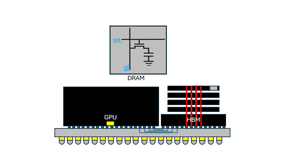
DRAM stores data in space-efficient 1T1C cells of one transistor and one capacitor. A charged cell where Vcell = VDD is equal to logical 1, and an empty cell is equal to logical 0.
In modern DRAM nodes, Cs is typically constructed as a tall pillar or trench dielectric to minimize surface area and typically on the order of 15 - 25fF. An NMOS transistor connects to the bitline and wordline.
This 1T1C cell is arrayed and connected horizontally through wordlines where a single wordline activation simultaneously accesses all cells in the row. This bitcell is connected vertically through bitlines that connect to sense amplifiers that data is read from.
During a read operation, the following operations occur:
-
The bitline is precharged and stabilized to a mid-rail voltage (1/2 * Vdd).
-
The bitline is disconnected from the supply rail and selected wordline is turned high
-
This causes charge to redistribute between the cell capacitance and the floating bitline capcitance.
-
Note that the bitline capacitance is typically 10 - 20x larger than the cell size itself.
-
The sensed voltage on the bitline is typically very small due to the capacitive divider ratio between them:
-
The sense amp is activated to read out the voltage.
-
Note that the actual process of "reading” the data is inherently destructive because all the charge is “lost” to generate the voltage.
-
This cell charge is “refreshed” from current rushing in through the sense amp.
-
The bitline requires a minimum refresh time to refresh the charge.
-
After the minimum refresh time, this wordline is driven back to 0.
Write operations follow a simpler set of operations than reads:
- The word line first is activated.
- The column write driver drives the bitline with high strength directly to full rail VDD or GND to charge or discharge the cell capacitor.
- Then the wordline is turned off.
DRAM is a volatile memory because the capacitor charge continuously leaks over time and data will be lost unless it is refreshed. Restoring sufficient charge requires periodic refresh commands issued by the memory controller to read every row and re-amplify its charge back to full rail before Cs drops below the sense amplifier's detection threshold. Frequent refresh commands at higher temperatures can cut into data BW by > 10%.
Most commercial DRAM relies on a tilted 6F^2 (3F * 2F) cell topology, where F refers to the feature size / design rule that the cell features scale off of, with future plans to transition toward 4F^2.
DRAM process nodes are fundamentally different from logic process nodes because they are optimized for two different features:
- Logic process nodes are 14–18+ metal layers for maximum connectivity with PnR tools. They scale performance by aggressively shrinking transistor gate lengths and gate pitches to maximize switching speed fmax.
- DRAM process nodes are 4–6 metal layers which is all they need to connect grid arrays. They are defined by the half-pitch (F) of the active memory cell array. They are optimized for maximum capacitive charge storage, ultra-low leakage, and low cost per bit.
DRAM and logic processes are generally incompatible because the high temperatures (600 deg) required to deposit and anneal high-k capacitor dielectrics destroy standard high-performance logic metal gates.
Key Components: Base Die and Core Die #
Next, we’ll examine the key features of two major components of HBM: The base die and core die.
Core Die
The core die consists of 4 - 16 DRAM dies, with efforts to push it up to 20. Each DRAM die contains multiple independent channels and up to 128 - 256 banks per die.
To fit 8 to 16 DRAM layers within JEDEC package Z-height limits (775 µm for HBM4), each core die is ground down to a 30 - 50um thickness before bonding with C2 bumps.
These layers are connected electrically with as many as 20,000 TSVs that also function as mechanical pillars. Due to mechanical stress surrounding the TSV, the immediate area around these TSVs is designated “keep-out zones” (KOZ) that DRAM cells are excluded to maintain consistent performance and yield.
HBM typically uses chip-on-wafer, chip-to-chip or wafer-to-wafer assembly techniques to stack DRAM dies one at a time. During assembly, individual DRAM dies are diced from their wafer, screened for defects, and then pick and placed one by one onto a base die wafer. This ensures only tested known good dies are added to the stack to protect overall yield.
There are two primary packaging technologies for stacking layers:
- Thermo-Compression + Non Conductive Film (TC+NCF). A NCF is first applied on the back of a wafer. Then, a precision bonder takes the DRAM die and applies downward force and localized heat. This causes a metallic bond to form from the microbumps melting through the softening NCF film
- This is primarily used by Samsung and Micron
- This technique handles warpage well because the solid NCF acts as a mechanical buffer, but is slow since each layer must be assembled one at a time.
- Mass Reflow + Molded Underfill (MR+MUF). Pioneered by SK Hynix, this process loosely stacks all dies together with temporary sticky flux that is then reflowed in one single pass where thousands of microbumps form simultaneously. Afterwards, a liquid epoxy molding compound is injected into the dies to act as the mechanical and thermal buffer.
- This single pass slashes HBM assembly times by 3 - 4x compared to TC-NCF, thus making SK Hynix the HBM workhorse with roughly 55% to 60% of market share
- However, this process is more sensitive to CTE and warpage during assembly.
Both TC-NCF and MR-MUF are so critical to South Korea that HBM stacking technology is legally classified as a critical national security asset where engineers face penalties for revealing the process secrets. The recipe for MR-MUF is perhaps the single most lucrative process secret in semiconductor packaging today.
More fundamental packaging process information, such as TSV formation, microbumps, and why hybrid bonding is generally challenging in practice can be found in my post:
Base Die
The base die acts as the primary bridge between the host memory controller on the xPU and the vertically stacked DRAM layers in the core die. The PHY contains 32 channels with 64 data I/O pins (DQs) per channel to deliver 2,048 I/Os.
In a typical HBM base die, a microbump PHY connects the host to the base die and drives these signals across the 2.5D silicon interposer microbumps. Signal TSVs populate the center while power and ground TSVs are distributed in a grid array across the base die footprint. Additionally, built-in self test (BIST) and direct access (DA) are included for debug and calibration.
Each channel uses short-reach single-ended (or pseudo-differential) drivers/receivers and forwarded clocking arranged in a grid format. This clock is distributed symmetrically. These drivers / receivers are optimized for layout area with a lot of functionality stripped out to fit all 2048 of them near the edge of the die.
In addition, the PHY contains two important error checking techniques utilizing parity bits:
- Link Error-Correcting Codes (ECC) - Corrects errors of data signals sent across the memory bus.
- Command/Address (C/A) parity checking - Detects errors in the instructions and destination addresses sent across the memory bus and asserts an error signal to the controller to retransmit the command frame
Both features are shifting from “nice to have” to “must haves” for denser, higher pin speed I/O with worse crosstalk and jitter effects.
During data communication, the xPU memory controller issues a read/write command into standard JEDEC frames. This packet consists of two things:
- **Address Vector:** Channel/pseudo-channel ID, target layer ID (C0-C16), bank group, bank, row, and column addresses.
- **Command Vector:** Operation code (e.g. ACTIVATE, followed by READ).
One critically important parameter that directly constrains memory BW is t_CCDR - the time between consecutive READ commands.
Here, two back-to back commands (RD_SID0 and RD_SID1) are issued to two different DRAM layers for data (DQ) travelling along two TSVs.
Notice how the read strobe (RDQS) differs across different layers in the stack. Time-of-flight, thermal mismatch, and die-to-die process variation across the DRAM stack naturally cause variations in read/write times, especially as stack heights get higher.
As a result, the system performance is affected by timing variation between stacked core die slices that cut into this t_CCDR limit.
One way to compensate for known mismatches is inter-die read delay. This uses high-resolution programmable delay lines to calibrate for known delays in the stackup. There are additional important features such as BIST and ABB that will be further discussed after the paywall.
Example Architecture: Samsung’s HBM4 at ISSCC 2026 #
A good example of a modern HBM4 architecture is from Samsung’s 2026 ISSCC 2026 paper.
In Samsung’s HBM, there are 32 PHY channels that contain a total of 2,048 total DQ bits across 32 channels, totaling 64 DQ bits per channel.
Each CH in the HBM stack contains a full local memory subsystem housing 16 banks per pseudo-channel (32 banks per full channel), along with their dedicated row/column decoders and sense amplifiers.
This structure delivers a massive total of 1,024 independently addressable banks with a bandwidth of 3.3TB/s and a cube density of 36GB with a 12 high stack.
The core die is fabricated using Samsung’s 6th-generation 10nm DRAM process and the base die is fabricated using a 4nm FinFET logic process.
Where Major Memory Makers Differentiate #
Before diving deeper into the intricacies of HBM, I want to highlight how each memory maker differentiates themselves.
- SK Hynix -The Advanced Packaging and HBM Yield leader. SK Hynix pioneered MR-MUF to deliver faster assembly throughput and superior thermal dissipation compared to traditional thin film-based stacking
- Samsung - The Vertically Integrated IDM. Samsung is positioned as a “one stop shop” as the worlds largest DRAM manufacturer and operates a memory division, logic foundry, and advanced packaging division, well suited for co-design.
- Micron -The Energy Efficiency & Node Architecture Innovator. Micron achieved ~30% lower power footprint per bit than competitors by optimizing deep ultraviolet (DUV/ArFi) multi-patterning for ultra-low I/O power consumption. This is enabled by their strategic decision to skip HBM3 and optimize HBM3e instead.
It is appropriate that each company in the HBM covered their strengths at Hot Chips 2026, though some covered them better than others.
In my view, there are four major problems with scaling HBM as it is. These are why, according to many semiconductor veterans like Pat Gelsinger, HBM is considered an architectural mistake in hindsight.