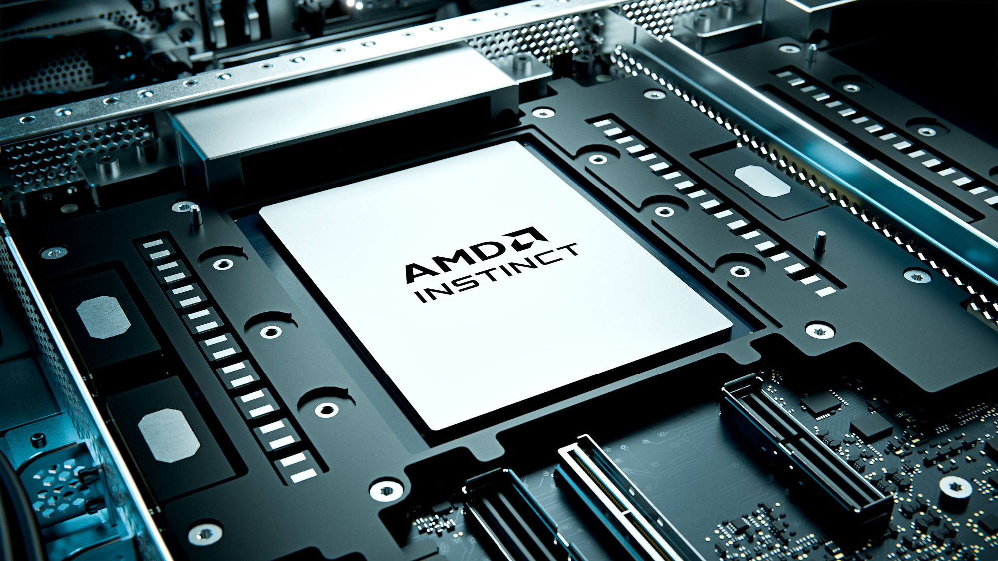
For the modern tech industry, the story of AI and the story of GPUs is often one and the same. The ultra-large, ultra-high-throughput chips have become a critical component of AI servers thanks to their combination of memory bandwidth and dense math throughput. And that role has only become more crucial in the last few years as AI servers have come into their own as a major product category, and as a major source of revenue within the tech industry.

For AMD, the effects of the AI boom have been nothing short of transformative for their server GPU efforts. Since launching their Instinct accelerator line almost a decade ago, AMD’s server GPU efforts have gone from a handful of sales to helping to drive data center sales to over 50% of the company’s total revenue. If not EPYC CPUs, then Instinct GPUs are the single most important product line at AMD in 2026.
But with that success comes the pressure to keep growing – and to keep improving their server GPU technology. To that end, as part of AMD’s 2026 Advancing AI event, the company’s GPU efforts took center stage, as AMD laid out its plans for the products and the new Helios rack-scale systems built around them.
The cornerstone of these new systems, and of AMD’s broader server accelerator product lineup for the next year, will be the Instinct MI455X. The latest and greatest from AMD, the Instinct MI455X is not only AMD’s fastest server GPU to date, but it marks the introduction of the radically revised CDNA 5 architecture, AMD’s biggest server GPU architecture overhaul in over a decade. With a combination of this architectural overhaul, TSMC’s cutting-edge 2nm process node, and a heavy emphasis on networking capabilities, AMD’s ambitions for its server GPUs have never been greater, or the performance higher.
Today we are taking a deep dive into the CDNA 5 architecture and the Instinct MI455X accelerator, to see what makes AMD’s latest server GPU tick, and what some of the many changes they have made to improve their performance while making the rack-scale Helios system possible. At the surface level, CDNA 5 does not bring much in the way of new high-level features, but this belies all of the major changes that AMD has made underneath. It is a GPU unlike anything AMD has done before, and it is the blueprint for all the server GPUs that will eventually follow. So, without further ado, let us dive right in.
AMD Instinct MI455X: By the Numbers #
Given all the changes that are at hand with the Instinct MI455X accelerator and the underlying CDNA 5 architecture, perhaps the best place to start is with a high-level look at the chip and its specifications.
The latest iteration of AMD’s server GPUs, MI455X is AMD’s prime CDNA 5 chip – a full-featured and fully-enabled implementation of the architecture. MI455X marks a number of important changes or additions for AMD’s server silicon, not the least of which is a radically altered core architecture, support for HBM4, and the move to TSMC’s first GAAFET process node: N2 (aka 2nm).
The combination of upgrades and overhauls promises to bring significant performance improvements for the MI455X versus its immediate predecessor, the MI355X. At a high level, AMD is touting a 4x peak improvement in matrix (tensor) performance with the all-critical FP4 and FP8 precisions. Meanwhile, peak compute performance for most other formats is set to double. And this is just for the raw compute throughput, never mind other improvements throughout the GPU architecture to improve throughput efficiency.
By the numbers, then, a single MI455X can process a bit over 40 PFLOPS of dense FP4 tensor operations or half that for FP6 and FP8. Like its predecessors, MI455X is designed to excel at tensor operations first and foremost, but traditional vector operations have not been left behind, either. The chip can chew through 315 TFLOPS of FP32 (or FP16) vector operations, roughly twice the rate of the MI355X.
Driving so much of these throughput gains is the simplest upgrade of them all: more transistors. Thanks in large part to the use of TSMC’s N2 process node for the compute dies, AMD is now able to assemble a chip with 320 billion transistors, a 72% increase from the previous generation. TSMC N2 in particular brings several perks here besides logic density, most notably better leakage control.
The CDNA 5 architecture also brings with it a huge revamp of AMD’s core GPU architecture. Essentially borrowing and enhancing the core compute architecture of AMD’s RDNA line of GPUs, which introduced a similar, SIMD32-based approach to ALU organization, CDNA 5 is the biggest change to AMD’s server GPU architectures since the Instinct line was launched almost a decade ago. The impact of the architecture change is going to be far-reaching, but the net result is that CDNA 5 should be a more efficient architecture overall, and as AMD tells it, a better fit to the kind of instruction flows being generated by AI workloads.
Feeding that new computing hardware, in turn, is a massive HBM4 memory subsystem that dwarfs even the chip’s theoretical compute gains. AMD has equipped the chip with 12 stacks of HBM4 memory, 4 more stacks than the MI355X. Which, thanks to all of the generational improvements in HBM4, gives the chip some 23.3 TB/second of memory bandwidth, 2.9x the bandwidth of the MI355X. As a result, the release of the MI455X will be one of those rare times where we see the amount of memory bandwidth per compute FLOP actually increase from one generation to the next (rather than decreasing, as is normally the case), which is one of the major factors helping to make MI455X more architecturally efficient than MI355X.
The new memory also brings with it capacity increases. At 36GB per stack, AMD can outfit MI455X with 432GB of local memory, some 1.5 times the capacity of MI355X. Surprisingly, given the importance of memory capacity to holding ever-larger AI models and context information, this is one of the few specs where MI455X does not double (or better) an MI355X spec. Though it is not for a lack of trying on AMD’s part, as evidenced by the use of 12 stacks of memory. At this point, all parties are bottlenecked by the slowed pace of DRAM density increases these days.
Next to memory bandwidth, I/O bandwidth is the other big bandwidth upgrade on MI455X. And in a lot of ways, it is the single most important aspect for unlocking AMD’s rack-scale ambitions. With 3.6TB/second of bandwidth available via Ultra Accelerator Link (UAL) lanes for scale-up fabrics, and more still via UAL, PCIe, and xGMI, MI455X offers over 4x the aggregate link bandwidth of MI355X. For this generation of AMD hardware, moving data was as important (if not more so) than computing it for the company.
There is a trade-off to all of these performance improvements, however: power. MI355X was already a toasty chip at up to 1400 Watts for a single accelerator. AMD has not even disclosed the power consumption of MI455X (ideally customers will buy it by the rack anyhow), but with a Helios rack consuming upwards of 245 kW of power – and with the majority of that going to GPUs – MI455X is thought to be somewhere north of 2 kW per GPU. Which, next to networking topology considerations, is one of the reasons that AMD is only putting four of them in a Helios compute tray.