When it comes to modern HPC and AI systems, high switch radix – meaning the number of ports you can hang off of a given switch ASIC – has become as important as low latency and high bandwidth.
Ideally, you would have a megaswitch that delivered all of this, one with an ASIC socket the size of a half dozen squared off 12-inch silicon wafers. But such a monster switch would present its own problems, which is why we are still breaking up the network just like we do compute and storage.
But just the same, getting a balance of these three different vectors – radix, latency, and bandwidth – is the job that switch chip designers are tasked with, and Innovium, the hyperscale Ethernet chip startup that was acquired by Marvell in August 2021, has been pushing the latency and bandwidth barriers since it was founded in 2015 and dropped out of stealth mode two years later. And with the new Teralynx T100, which will start sampling any day now, Marvell’s switch ASIC team is pushing the limits to the hilt. By doing so, Marvell is likely to expand the use of the Teralynx chips and switches by the hyperscalers and cloud builders, and may even get some traction at the AI model builders looking for high bandwidth, high radix, and low latency Ethernet for their scale out and scale up networks.
The Teralynx chips have been on a tear since the coronavirus pandemic hit in 2020. The formerly independent Innovium shipped over 1 million 400 Gb/sec Ethernet ports with a mix of its Teralynx 7 and 8 chips in 2020, and two years later Marvell pushed the Teralynx ASICs into mass production, with ASICs ranging from 12.8 Tb/sec to 51.2 Tb/sec of aggregate bandwidth.
By 2023, Marvell had shipped over 5 million 400 Gb/sec ports, which works out to somewhere well north of 300,000 switches. By last year, Marvell had sold more than 20 million 400 Gb/sec ports, which is probably somewhere around 1.25 million switches, thanks in large part to the delivery of the 51.2 Tb/sec Teralynx 10 ASIC that ramped in 2024 using 5 nanometer processes from Taiwan Semiconductor Manufacturing Co.
This time around with the Teralynx T100, Rishi Chugh, general manager of the Network Switching Division of Marvell, tells The Next Platform that it is pushing the limits hard, making a monolithic switch ASIC that is up against the reticle limits and that is employing TSMC’s 3 nanometer process, and probably its N3E refined variant if we had to guess.
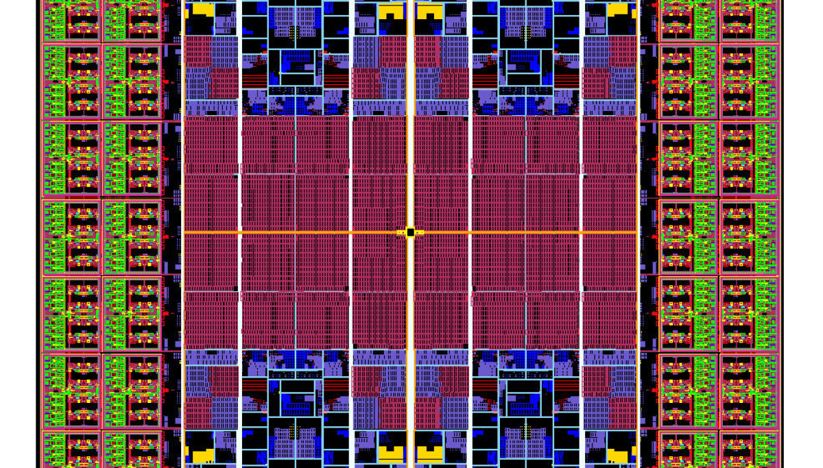
We very rarely get a die shot of a switch ASIC these days, but Chugh made sure we got one for the T100:
Pretty, isn’t it?
At 100.4 Tb/sec of aggregate bandwidth and using 224 Gb/sec SerDes (which is cut down to 200 Gb/sec after signaling overhead is taken off), there are 512 SerDes wrapped around the outside of the packet processing engines and SRAM cache used in the T100. That red area is the SRAM, and there are clearly four blocks of packet processing engines.
I count 76 SerDes blocks – 18 on each side left and right, and 18 on the top and bottom plus four in each corner. If each block is four SerDes, then that works out to 608 SerDes, and if you assume an 84 percent yield on these blocks, you get 512 working SerDes.
Chugh says that by sticking with a monolithic die and not breaking the SerDes into chiplets, the T100 has 25 percent lower power consumption. There is that yield issue with a big monolithic chip on a fairly new N3 process, of course, which is why the actual SerDes count on the chip is 19 percent higher than what the spec sheet says. But if you want to drive performance and lower power, you make a more expensive chip.
Clearly in this AI era, money is not yet a limiting factor. . . .
The typical power consumption of the T100 chip will be under 1,000 watts and significantly the chip has a port to port hop latency of only 420 nanoseconds. That is not as low as InfiniBand can get at the same port speed – about 130 nanoseconds – but with some extra engineering Marvell hopes to get the latency down to the middle 300 nanoseconds range, which is low enough that the T100 can support the ESUN scale up memory sharing protocol for AI accelerators, which is going to become an alternative to Nvidia’s NVLink protocol and its NVSwitch memory fabric among the XPUs of the world.
The T100 also supports the Ultra Ethernet Consortium protocols, importantly the adaptive routing functions that make scale out networks work well with tens to hundreds of thousands of XPUs. And like the Teralynx 7 and Teralynx 10 chips before it, it can run the open source SONiC Linux-derived network operating system that was originally created by Microsoft as well as the homegrown NOSes created by the hyperscalers and cloud builders that Innovium was originally targeting as its initial customers.
As you can see, you can bundle up those 512 working SerDes in a number of ways. If you have one SerDes driving one port, you get 512 ports running at 200 Gb/sec. You can do 256 ports at 400 Gb/sec, 128 ports at 800 Gb/sec, and 64 ports at 1.6 Tb/sec. This is still nowhere near the bandwidth Nvidia is driving with NVSwitches, but the NVSwitch also has low radix so you end up chaining them together anyway.
Perhaps most importantly for Marvell, the Teralynx T100 will come with a variety of different wiring options.
If you just want a normal BGA packaging of the chip, you get a switch that looks like this: The two BGA reference platforms are aimed at delivering 64 ports running at 1.6 Tb/sec in a 3U form factor. The first version supports the Open Rack v3 form factor from the Open Compute Project, which supports bus bar power supply and which has a 21-inch wide form factor. This machine implies strongly that Meta Platforms might be using this T100 switch ASIC. The BGA reference platforms also includes a normal 3U form factor with 19-inch wide chassis with normal AC power supplies. Both of these BGA reference switches will start sampling in Q4 2026.
For those of you who are not ready to go all the way to co-packed optics (CPO), there is a co-packaged copper (CPC) variant and here are two reference platforms for that: The one on the left is a 2U switch that supports 64 OSFP ports running at 1.6 Tb/sec and has CPC out to the F-OSFP ports. The one on the right is a 1U switch that looks to have only 24 ports.
There is a NPO version that can drive signals directly out of the SerDes, which is not shown, and of course there is a proper CPO version for those who want to go that route:
The CPO variant of the T100 reference platform is an Orv3 design as well and has a DC bus bar design but also has an AC power supply as an option. It has a Compute on Module Express (COMe) control plane, which supports either X86 or Arm CPUs. This initial CPO design has a mix of air and liquid cooling, but the expectation is that the T100s will be mostly liquid cooled with the CPO option.
Switches based on the T100 are expected to offer the following capex and opex total cost of ownership benefits:
It is not clear what a volume deployments mean, but it is probably tens of thousands of switches to get that $200 million in TCO savings cited above. That scale is not a big deal in the GenAI era.
Marvell expects to have the ESUN switch based on a variant of the T100 out in the second half of 2027, and the rumors out there on the street are that Microsoft and Meta Platforms will be big supporters of ESUN. Marvell is also planning a UALink switch for the first half of 2027.