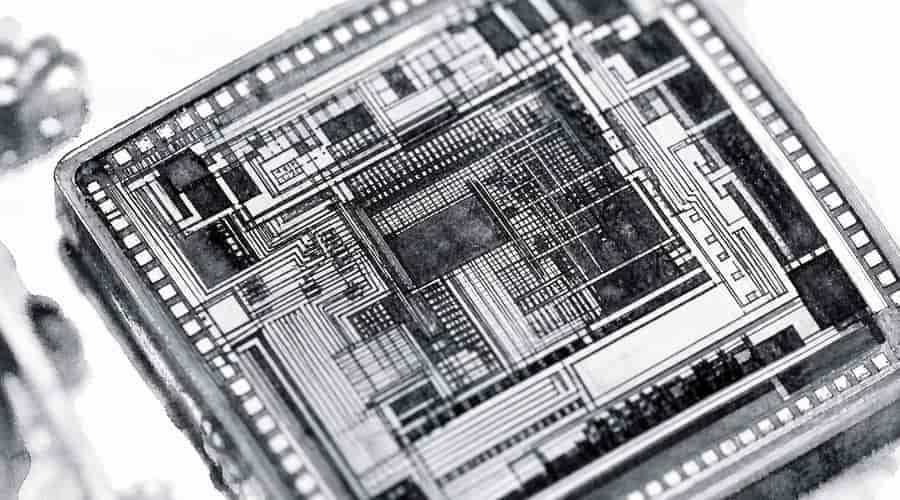
IBM has unveiled the world's first sub-1 nanometer chip technology, a 0.7nm nanostack design that doubles transistor density over its own 2nm benchmark and is built explicitly for the data demands of AI workloads.
The numbers IBM published today are hard to sit with. A chip the size of a fingernail. Nearly 100 billion transistors packed onto it. That's roughly twice the density of IBM's 2nm design from 2021, which was itself considered extraordinary at the time. The new 0.7nm node, also described as 7 angstroms, uses what IBM calls a nanostack architecture: a three-dimensional, vertically stacked, nanosheet-based transistor design that staggers layers to extract performance and energy efficiency from each one independently. IBM says the architecture delivers 40 percent SRAM scaling gains and that it projects at least a decade of continued roadmap from here.
That last claim is the one that matters most. Moore's Law has been declared dead so many times that the announcement barely registers anymore, but IBM's 0.7nm result is genuinely different in kind, not just degree. Moving below 1nm means operating at the angstrom scale, where individual atoms start becoming legible features on the chip surface. That IBM has demonstrated a working path through that territory, with a specific architectural innovation and not just a materials tweak, is a real milestone.
The technical case for the nanostack design is specific. Previous nanosheet transistors stacked sheets horizontally. IBM's approach stacks them vertically and staggers them, which lets engineers tune the material combinations in each layer independently. The practical result is that you can optimize performance and power draw at the transistor level rather than making one compromise for the entire chip. IBM is pointing directly at AI inference as the target use case: the architecture is built to handle the high-bandwidth data movement that large model inference demands, and the 50 percent performance gain or 70 percent energy efficiency gain over 2nm node chips is cited explicitly in that context.
That framing is deliberate, and it puts IBM in direct conversation with Nvidia, which currently controls AI inference silicon with a grip that most competitors have found impossible to loosen. Nvidia's H100 and B200 series aren't losing design wins, and the company's CUDA ecosystem is a moat that doesn't shrink when a competitor announces a process node. But if IBM's density claims hold at volume production, the competitive math for AI chips shifts. More transistors per millimeter, less power per inference, smaller form factor: those are the exact levers that hyperscalers and enterprise buyers are pulling on right now as inference workloads scale past what anyone budgeted for.
Frankly, the gap between IBM Research announcements and shipping silicon is the part of this story that deserves the most scrutiny. IBM's 2nm breakthrough from 2021 was real science. It also spent years in lab form before any meaningful commercial volume materialized, and it was eventually handed to partners to commercialize rather than manufactured by IBM itself at scale. The 0.7nm announcement follows the same pattern: a genuine research result with no committed production date attached to it.
The Rapidus question #
Rapidus is the most likely commercial path for IBM's advanced node work. The Japanese chipmaker, which is chasing 2nm pilot production at its Chitose, Hokkaido facility with IBM engineers on site, landed $1.7 billion in February 2026 to fund that push, with commercial wafers for Fujitsu targeted for 2027. IBM has dispatched roughly 10 engineers to the Rapidus fab, and the two companies have indicated a deepening partnership on sub-1nm development. That's the supply chain story here: not whether IBM can demonstrate the physics, which it clearly can, but whether Rapidus can turn IBM's research into volume production without the delays and funding crunches that have shadowed it since its founding. In March 2026, Digitimes reported that Rapidus scaled back its US R&D presence early, raising fresh questions about its timeline and capital runway.
None of that diminishes what IBM announced today. The nanostack architecture is a structural innovation, not a marketing rebranding of an existing process node, which is a distinction the semiconductor industry has been guilty of blurring for years. IBM is also not alone in pursuing sub-1nm territory: TSMC and Intel are both working toward similar nodes, and Lam Research announced a collaboration with IBM in March 2026 specifically targeting High-NA EUV dry resist integration for sub-1nm logic. The competitive pressure is real, and IBM's result means it's a participant in that race rather than a spectator.
For anyone betting on the AI chip market over the next several years, the 0.7nm announcement is a signal that the density ceiling is not where the pessimists said it was. The harder question is whether the companies that can manufacture at this node will be the ones that get the chips into the data centers where inference actually runs. IBM has solved the physics. The production problem is still open. Also read: Amazon raises its India bet to $48 billion as Big Tech turns the subcontinent into an AI proving ground • OpenAI quietly upgraded every free ChatGPT user to a smarter model and the competition should be worried • PropMIS Is Building HOA Management Software Where AI Was There From Day One