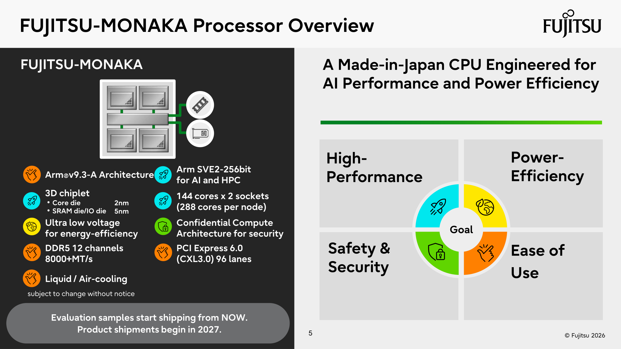
After a short break, we are back for the second set of CPU sessions at Hot Chips 2026. Leading the second group of presentations is Fujitsu, who has come to this year’s show to dive deeper on Monaka, their next-generation server CPU. The successor to Fujitsu’s initial Arm-based CPU, the A64FX, the Monaka is designed to be a cutting-edge CPU aimed at the data center market. The company has previously disclosed that the chiplet-based CPU will offer up to 144 CPU cores, and will utilize 3D stacked chiplets to bring the whole chip together.
Please note, we are covering this live, so please excuse typos.
Fujitsu’s Arm-based Monaka Data Center CPU at Hot Chips 2026 #
While Fujitsu’s earlier A64FX CPU was primarily seen in the Fugaku supercomputer, Fujitsu has greater ambitions for the Monaka. Riding the surging wave of Arm-based CPUs in servers and data centers, the company is positioning the Monaka as a CPU built for modern AI workloads. As well, the company is focusing heavily on energy efficiency, which has quickly become a constraining factor in data centers. According to Fujitsu, the role of CPUs in AI systems is expanding. Agentic workloads are pushing CPUs like never before, as CPUs are doing far more than just coordinating GPUs these days.
Monaka’s value proposition is that AI adoption is currently constrained by power limitations, which Monaka addresses by running at ultra-low-voltages for maximum efficiency. Combined with that, Monaka is designed to be a better fit for modern workloads, as well as meeting the needs of sovereign AI.
Monaka is an Armv9.3-A architecture design. The chip uses 256-bit SVE2 SIMDs, which is a rarity in the Arm space as most designs have been 128-bit SVE2 (the exception being the 512-bit A64FX, of course). The core chiplet is built on a 2nm process, while the SRAM and IO dies are made on 5nm. There are 12 channels of DDR5 memory, and 144 CPU cores per chip (with the ability to go up to 2P per node).
Looking a bit at the history of the semiconductor industry, 2nm is going to deliver a huge boost in chip density and performance thanks to its use of GAAFETs. But it is not the optimal solution for all parts of a chip, which is why they are using chiplets built across multiple process nodes.
The core die is made on TSMC’s N2P process node. Meanwhile the SRAM and I/O dies are made on TSMC’s N5 process node. N2P is used for less than 30% of the total silicon area; most of the chip is made on N5. By splitting things up in this fashion, Fujitsu is able to accelerate their time-to-market for what is a cutting-edge chip.
The chiplet architecture means using die-to-die hybrid bonding between the stacked elements. The core die sits on top of the SRAM die, and then the silicon interposer below that.
Fujitsu also gave low dropout regulators (LDOs) a particular focus here, as these are analog circuits that do not shrink well with smaller process nodes. All of this helps them hit a better level of cost-versus-performance.
Thanks to one of the core rules of chip operation, that power is a product of capacitance, frequency, and the square of the voltage, the biggest power consumption gains can be found by reducing a chip’s voltage. To that end, Fujitsu has put a heavy emphasis on running Monaka at ultra-low voltages to maximize its energy efficiency. There is a strong emphasis here on how this is a non-standard way of designing chips, and required special design tools to help accomplish it.
Fujitsu says that they are running the voltages at around 30% lower than similar designs, but they are not disclosing the specific voltages they are running at.
Talking a bit more about Monaka’s core design, and reiterating how Monaka uses a wider-than-average 256-bit SVE2 execution unit. The company believes that this is the best fit for the data center market, who could benefit from a wider SIMD, but not the ultra-wide 512-bit SIMD used by the A64FX.
There are dual SVE2 units in each core. These are paired with a duo of 256-bit load/store units in each core.
Looking a bit more closely at power optimization techniques, Monaka implements a floating point register cache to help cache data in programs with high temporal locality. Which happens to be a lot of GEMM workloads.
Meanwhile to optimize power consumption with reads, Monaka can bypass the predicate register in some situations.
Another power optimization is to reduce energy usage with vectors that are narrower than 256-bits wide. In this case they can be masked off as 0s, reducing the power consumption on that part of the SIMD.
As for performance considerations, Fujitsu has given extra attention to being able to fully utilize the 256-bit SIMD unit. A combined gather instruction is particularly helpful in HPC applications.
As for memory access and NUMA nodes, Monaka offers three different configurations: 1, 4, and 8 NUMA nodes. With 144 cores, 36 cores, and 18 cores respectively. The 1 node configuration is for large memroy applications, while 8 nodes factors high throughput.
Each NUMA node can be split up into two LLC regions. Monaka supports up to 63 MPAMs, which is independent of the NUMA nodes.
Confidential computing support is also baked into Monaka as part of the Arm confidential compute architecture. This requires co-design between the hardware, the firmware, and the software stack running on top in order to support all of the necessary features.
And looking at the software ecosystem in a bit more detail here, Fujitsu is making heavy use of open source software here. But they are also tapping bits and pieces of NVIDIA’s open source software stack to make for a complete ecosystem.
Monaka will be offered in two SKUs: a high-performance SKU and a high-efficiency SKU. Both have 144 cores, but the high performance SKU will operate at 500 Watts, versus 350 Watts for the high-efficiency SKU. This brings the base frequency up from 2.1GHz to 2.9GHz, and an estimated performance of almost 50% higher.
Monaka is set to arrive in 2027. Meanwhile the company is already in the process of developing Monaka-X, which will be a faster chip fabbed on a 1.4nm process, and which will incorporate NVLink Fusion support for better connectivity to NVIDIA (and other NVLink) accelerators in the futre.