At the 2018 [International Symposium on Computer Architecture], and
John Hennessy delivered their
David Patterson[Turing]Lecture: .
"A New Golden Age for Computer Architecture"In the 1980s, when * Hennessy* and
did their Turing Award-winning research,
Patterson single-threaded CPU performance grew 52% a year. By 2018, with the end of
and
[Moore's Law](https://en.wikipedia.org/wiki/Moore%27s_law)*, the rate was 3%.*

[Dennard Scaling](https://en.wikipedia.org/wiki/Dennard_scaling)There was a need for * domain-specific architectures* (DSAs). Their worked example was Google's
, already in production: 29× the throughput of a CPU on neural-network inference, at 80× better energy efficiency. The closing prediction:
TPU v1 "the next decade will see a Cambrian explosion of novel computer architectures." This prediction came true. Today, we now have dozens of architectures in serious development. * GPUs*,
,
TPUs*,*
LPUs*,*
NPUs*,*
DPUs*,*
ASICs*,*
wafer-scale engines*,*
reconfigurable dataflow*,*
neuromorphic*,*
photonic*. Particularly, these architectures focus on compute for*
analog*.*
AI The architectures that have won real deployment so far: * GPUs* (NVIDIA, AMD),
(TPU, Trainium), the systolic-array accelerators*, and the*
Cerebras Wafer-Scale Engine*.*
Groq LPU* NVIDIA* is the clear frontrunner;
follows, with 6 GW commitments from both
**AMD**[OpenAI](https://openai.com/index/openai-amd-strategic-partnership/)and

[Meta](https://www.amd.com/en/newsroom/press-releases/2026-2-24-amd-and-meta-announce-expanded-strategic-partnersh.html).
train Gemini and will
**TPUs**[serve Anthropic with up to a million chips](https://www.anthropic.com/news/expanding-our-use-of-google-cloud-tpus-and-services); Anthropic also runs Claude on

[over a million](https://techcrunch.com/2026/03/22/an-exclusive-tour-of-amazons-trainium-lab-the-chip-thats-won-over-anthropic-openai-even-apple/).
chipsTrainium
Cerebrasnow serves OpenAI inference; the was
Groq LPUfolded into NVIDIA via a $20B acquihire. This post aims to survey these varying approaches - their philosophy, architecture, scaling methods (scale-up and scale-out), and software stack (how you program the chip).
The Problem
AI compute is dominated by * matrix multiplication*. A transformer is a sequence of matmuls:
,
Q/K/V projection*,*
attention*,*
output projection*- interleaved with element-wise ops: normalisation, activation, residual adds.*
FFN[Training]a frontier model performs multiply-accumulate operations (matmuls are a sequence of multiply-accumulates).
The shape of those matmuls depends on the workload. pushes a batch of sequences forward through every layer, backpropagates the loss, and updates the weights, with thousands of tokens flowing through the same weight matrix at once.
[Training] is the prompt-ingestion phase of inference: the full input sequence projected through the model in a single pass, before the first output token has been produced. Both training & prefill stack many tokens against the same weight matrix, so each layer's math is a large
[Prefill]*multiply (GEMM), with high*

**matrix-matrix**[arithmetic intensity](compute-bound).
is autoregressive: the model emits one token at a time, each conditioned on every token before it, and token
[Decode]N+1cannot begin until token Nhas been produced. Only one token gets projected per step, so every matmul becomes a
product (GEMV). Producing one token requires a full pass over every weight in the model, plus a full read of the
matrix-vector[KV Cache]for attention. Arithmetic intensity drops by orders of magnitude versus
[prefill]. Inference systems recover some of that intensity by batching tokens to promote those GEMVs back to GEMMs: stacks many users'
[continuous batching]

[decode]steps,
stacks K drafted tokens per request and verifies them in one pass, and
[speculative decoding]folds the same trick inside the model itself. This achieves higher utilisation of the matmul units, and pushes up the Ops/B. For continuous batching, each user's request still reads its own
[multi-token prediction][KV Cache], so long-context decode shifts from weight-bandwidth-bound to KV-bandwidth-bound. The architecture problem here is * moving the numbers* to where the matmuls happens fast enough. This is known as the
: compute has scaled exponentially, memory bandwidth has not.
[memory wall]Each architecture proposes a different strategy for winning the data-movement game. Understanding a chip reduces to four questions: where does data live, how does it move to the compute units, what do the compute units look like, and how do chips talk to each other at scale.
NVIDIA GPU
The NVIDIA GPU is a * massively parallel processor*. The philosophy is that a programmable chip with thousands of threads, orchestrated by a host CPU and exposed through
, is the right machine to run
CUDAworkloads. Each generation adds acceleration primitives onto programmable parallelisable* without changing the programming model. The same chip trains transformers, serves inference, renders graphics, and runs scientific simulation (*
Streaming Multiprocessors*).*
accelerated computing#### Genealogy
[unified shaders]and the

[SIMT execution model].

[warp schedulers], IEEE-754

[FP64].
Architecture
An NVIDIA GPU is a group of * throughput-oriented cores, a deep memory hierarchy to keep them fed, + just enough scheduling silicon to keep thousands of threads in flight*. The cores are
, replicated 100+ times per package: 80 on
Streaming Multiprocessors[V100], 108 on
[A100], 132 on

[H100], 148 on

[B200], 160 on

[B300], 224 on

[Rubin]. Inside every SM sits the same recipe: four
, each with its own
SM Sub-Partitions*,*
[warp scheduler]*, 16k×32-bit*

[dispatch unit]*, scalar*

[register file]*lanes, a*
[CUDA Core]for transcendentals, and a private port into the SM's
[Special Function Unit]. The four partitions share an
[Tensor Cores][L1/shared-memory]block, and the

[TMA]. Threads are grouped into
of 32 that execute in
[warps][SIMT]lock-step; dozens of resident warps per partition let the scheduler hide memory/arithmetic stalls by switching between them.
Compute
are the original compute throughput, and for AI they still own everything that isn't a matmul: activations, residual adds, normalization, address arithmetic. But, a transformer block is ~99% matmul FLOPs, so the overwhelming compute throughput comes from the
[CUDA Cores] .
[Tensor Cores]These cores execute * fused matrix multiply-accumulate* on small matrix tiles, The full matmul is broken into output tiles: to produce one output tile, a kernel walks the shared inner dimension , drawing from a row-strip of the left input matrix and from a column-strip of the right, and folds each partial product into a running accumulator. holds the partial sum so far, is the updated value carried into the next step. After the inner loop completes, is one finished tile of the full output matrix; the whole matmul is built from many of these tile
[MMAs]. Tile shapes are written M × N × K, is the output tile size, and is how much of the inner dimension the instruction contracts over in one fire; the rest of the matmul's axis is walked by the kernel's inner loop. The accumulator is sticky across that loop: each MMA's output becomes the next MMA's input , so the equation is really in place: successive instructions fold their partial products into the same storage until the K-axis is fully walked.
[V100]'s first-gen unit (8 per SM) ran a warp-level 16×16×16 FP16 [MMA]. [A100]'s 3rd-gen unit added [TF32], [BF16], FP64 matmul, and 2:4 [structured sparsity]. [H100]'s 4th-gen unit added native [FP8] and pulled the abstraction up from a warp to a : 128 cooperating threads firing an asynchronous
[warp group] [at 64×256×16 shape that runs in the background while the issuing warps load the next tile.]
wgmma
[B200]'s 5th-gen unit went further still: a of 256×256×16 with operands split across a pair of SMs, native
[two-SM MMA][FP4], and a dedicated 256 KB scratchpad per SM that holds accumulator tiles instead of bleeding into the register file.
[Tensor Memory (TMEM)][Rubin]'s 6th-gen unit extends FP4 throughput, adds native FP6, and pairs with a 3rd-gen

[Transformer Engine]that does adaptive
[NVFP4]micro-block scaling in hardware, keeping the per-tile quantization metadata on the
[Tensor Core]path, rather than through the
[CUDA Cores]. What stays constant across all six generations is that the matmul lives inside the * thread/warp hierarchy*, but the number of threads it takes to
issueone has shrunk, and the issue itself has decoupled from execution.
[Volta]'s
mma.sync
is warp-[collective]and synchronous: all 32 threads in a [warp]execute it together, each lane holding register fragments of A, B,
and the accumulator D, and the warp blocks until it completes.
[Hopper]'s

[widens the issuer to a]
wgmma.mma_async
[warp-group]of 128 threads, moves B into a

[shared-memory descriptor](A becomes optional: either registers
ora descriptor, kernel's choice), and
returns immediately: the matmul runs in the background while the warp-group queues the next tile, with completion tracked via
wgmma.commit_group
/ wgmma.wait_group
.[Blackwell]'s tcgen05.mma
completes the migration: A joins B in [shared-memory descriptors] (or A comes from [TMEM] directly), and the accumulator D lands in TMEM rather than the register file. With every operand off the lanes, there is no per-thread state for an issue to coordinate, so a single thread fires the instruction and returns immediately, with completion signalled by an [ mbarrier] the consumer warp waits on. The rest of the warp, and the issuing thread itself, is free for other work in the meantime. A
scales the same model across two SMs: one thread on each SM in a paired cluster issues coordinated
[CTA]-pair variant[MMAs]that share operands across the pair, composing the

[256×256×16 two-SM tile]under the same async/
mbarrier
completion, just promoted to a cluster-level barrier so the pair stays in step.The matmul has grown bigger and lighter on the issuing threads at the same time: an instruction that started as 32 lanes acting in lockstep is now closer to a single [descriptor-driven command], dispatched from inside the warp model but no longer executed by it.
That decoupling is what makes transformer attention kernels efficient on a GPU. The warp can run softmax, apply a mask, or pre-load the next tile while the matmul is in flight; the overlap of matmul and the surrounding element-wise work is the structure of every modern attention kernel ([FlashAttention-3], FA4), and it depends on the matrix instruction not blocking the warp.
Memory
The on-chip hierarchy is * hardware-managed caches at every level, with software hints layered on top*. Off-chip is
: 32 GB
[HBM][HBM2]on V100, 80 GB

[HBM3]on H100, 192 GB

[HBM3e]on B200, 288 GB on B300, 288 GB

[HBM4]on Rubin. A chip-level
sits between HBM and the SMs: 6 MB on V100, 40 MB on A100, 50 MB on H100, 60 MB on B200 (split into two 30 MB banks across the
L2 Cache[two-die package], with locality-aware [residency controls]so that hot tiles can be pinned to the near die). Inside each SM, 256 KB of unified
is partitioned at kernel launch between hardware-managed L1 and a programmer-controlled scratchpad. The register file is another ~256 KB per SM, sliced four ways across the partitions.
[L1/SMEM]Blackwell adds a fifth tier: , 256 KB per SM dedicated to
[TMEM] [MMA]accumulators and addressed only by the Tensor Core, pulling the operand-residency pressure out of the general register file.
Movement between tiers has been progressively decoupled from the warp. Pre-Ampere, a tile was synchronous: each thread issued its own global load, the warp blocked until every fragment landed in registers, and a second pass copied them to shared memory; every tile burned warp lanes on address arithmetic and on the wait. [Ampere] introduced : per-thread async copies HBM → SMEM that bypass registers entirely, with the warp committing groups of in-flight copies and waiting only when the consumer needs the data.
cp.async
[Hopper]replaced that with the , a dedicated DMA engine: one thread submits a multi-dimensional tile descriptor (base address, leading dimension, swizzle), the engine handles all the address arithmetic and writes into shared memory, and completion is signalled by an
[TMA][. The whole warp is freed from load issue and address math; the kernel just queues descriptors. TMA also supports]
mbarrier
cluster-level multicast: one HBM read fans out to every SM in a
[thread-block cluster], turning what used to be N separate loads into one.
[Blackwell]extends TMA again: direct loads into [TMEM], so accumulator tiles stream in without staging through SMEM. The trajectory is one less thing the warp has to do per tile, generation after generation.
Warp Specialisation
The Hopper-era programming idiom is : inside one block, some warps act as
[warp specialisation]

*that issue back-to-back*

**producers**[TMA]loads; others act as
that fire
consumers[on freshly-arrived tiles. Synchronisation between them is no longer the old SM-wide]
wgmma
__syncthreads()
barrier; it is (memory barriers in shared memory) and asynchronous transaction barriers attached to TMA completions, allowing fine-grained producer/consumer handshakes at warp granularity rather than block granularity. The pattern that has become the reference for every modern attention kernel (
mbarrier
[FlashAttention-3], ping-pong GEMMs, the Blackwell
CUTLASS[FA4]kernel) is the same recipe: a TMA-driven producer pipeline feeds a wgmma consumer pipeline through shared memory and TMEM, with mbarrier handshakes and
(Hopper+) tying multiple SMs into one cooperative compute unit so that the two-SM MMA of Blackwell composes naturally on top.
[thread-block clusters]##### Numerics [FP32] was the historical default; Volta brought with FP32 accumulate and the
[FP16]

[loss-scaling]tricks that made it trainable; Ampere added

*(FP32 range, FP16 mantissa, drop-in for FP32 matmul),*

[TF32]*, and 2:4*
[BF16]that doubles effective throughput on pruned weights. Hopper introduced native
[structured sparsity]*in both*

[FP8][E4M3]and

[E5M2], paired with the
which auto-scales activations layer-by-layer to keep them inside FP8 dynamic range. Blackwell halved precision again with
[Transformer Engine]and shipped [FP4](block-level shared exponents that recover most of the accuracy lost at FP4), together with a 2nd-gen Transformer Engine that retargets the auto-scaling pipeline to FP4. Rubin's 3rd-gen Transformer Engine adds
[microscaling MX formats](NVIDIA's tightened FP4 variant) and native [NVFP4]with more aggressive sparsity. The chip layout itself is now part of the numerics story: B100/B200/B300 are
FP6* stitched by a ~10 TB/s*
[two reticle-limit dies]link and presented to software as one logical GPU, with 8 HBM stacks on the package; Rubin extends the chiplet recipe to dual-die at ~336 B transistors with 8 HBM4 stacks. Every generation buys roughly 2× per-watt throughput by cutting bits in half and restoring accuracy with a finer-grained scaling scheme, and increasingly, by bonding more silicon into the package.
[NV-HBI]##### Bets
The workload is a moving target (attention variants, novel model architectures), so keep every block programmable and let the developer writeBet 1: Programmability.CUDA. Even the specialised units are exposedthroughthat model rather than as fixed-function blocks.Latency is unpredictable and data-dependent, so hide it not with a static schedule but with massive thread overcommit, up to 64 resident warps per SM, with the hardwareBet 2: Hide Latency with Massive Multithreading.[warp scheduler]picking a ready warp every cycle.The matrix unit is the overwhelming compute throughput, but it must live behind the same warp/thread abstraction that everything else uses, so wrap it inBet 3: Warp-wrapped Matmul.mma.sync
→wgmma
→tcgen05.mma
- rather than expose it as a fixed-function pipe. This enables a single kernel to fuse matmul, softmax, and element-wise ops in one pass.Make the memory hierarchyBet 4: Async Memory Hierarchy.[explicit]and[programmer-managed]rather than[implicit]and[compiler-scheduled]. Keep the[L2 cache], but expose[SMEM]and[TMEM]as named scratchpads, and layer async machinery on top:[TMA]for bulk copies,[TMEM]for the matmul accumulator,for the producer/consumer handshake. The hierarchy is
mbarrier
[software-pipelined]inside a programmable kernel, not statically scheduled by a compiler against a known-latency scratchpad.Every transistor spent on a warp scheduler, register-file, or coherent cache is a transistor not spent on aBet 5: Amortised SIMT Tax.[MAC]; accept the tax, and pay it down two ways: a Tensor Core now big enough that the SIMT machinery is amortised across a much larger MAC count, and units like TMEM trading away some general-purpose flexibility for MAC density.
Scaling
There are two regimes for scaling: and
[scale-up] .
[scale-out]AI infrastructure uses both: bandwidth-hungry [collectives] ([tensor parallelism], [MoE expert routing]) stay inside the scale-up domain; [data parallelism] and [pipeline parallelism] cross the scale-out fabric.
Scale-up
The scale-up stack is plus
[NVLink] .
[NVSwitch][NVLink]implements a between GPUs, so a load or store on one GPU can target another GPU's
cache-coherent fabric[HBM]with the hardware handling address translation and coherence. But
[NVLink]by itself is point-to-point: one link connects exactly two chips.

[NVSwitch]is a dedicated
chip that every GPU connects to, routing traffic so every GPU can simultaneously communicate with every other at full
[crossbar][NVLink]bandwidth,

[non-blocking]and

[all-to-all].
Together they defined the 8-GPU baseboard, pairing eight
[HGX]

[H100]

[SXM]modules with

[x86]hosts (

[AMD EPYC]or

[Intel Xeon]) over

[PCIe Gen5]. Hopper also shipped a

[Grace]-paired form: the
bonded one
[GH200 Grace Hopper Superchip][Grace]ARM CPU to one

[H100]over
at 900 GB/s, eliminating the
[NVLink-C2C][PCIe]host-device hop. Modules scaled up into pairs and rack-level
[GH200]NVL2*. Blackwell makes the pairing the default. The*
[GH200]NVL32*module fuses one*

[GB200][Grace]with two B200s over

[NVLink-C2C], and
stitches 36 of them into a single liquid-cooled scale-up domain: 72 GPUs, 36
**NVL72**[Grace]CPUs, 13.5 TB of

[HBM]and 17 TB of
[LPDDR5X]as one flat, coherent address space. Rubin steps this in two.
ships in 2026 as a Rubin-generation refresh inside the same
NVL144[Oberon]-class rack: 72 Rubin packages, badged as 144 GPUs under NVIDIA's new die-counting convention, with
[HBM4]and NVLink 6 doubling per-package bandwidth. The actual rack-scale jump is Rubin Ultra in 2027:
packs 144 four-die Rubin Ultra packages into the new
NVL576* chassis for 576 GPU dies in one coherent domain.*
Kyber That density is held together by . NVL72's NVLink fabric runs over 5,184 cables blind-mated through a backplane (~2 miles of cabling per rack, no
[passive copper]

[in-cable retimers], the

[SerDes]living on the GPU and

[switch ASICs]themselves), carrying ~130 TB/s of
[all-to-all]bandwidth across the 72 GPUs. NVIDIA estimates the copper choice saves roughly 20 kW per rack against an optical equivalent that would have needed
[pluggable transceivers]on every link. Copper is what makes
rack as one GPUeconomically practical: at sub-2-metre runs it still wins on power, cost, and signal integrity per dollar; beyond that, the bits have to go on glass.
NVL144 stays inside Oberon and copper continues to work because the package count (72) is unchanged from NVL72; the cabling doesn't have to lengthen, just transmit faster on Gen 6 SerDes. [Rubin Ultra]'s NVL576 holds the same copper line by reshaping the rack: the new * Kyber* form factor is roughly twice the height of Oberon and packs all 576 GPU dies into one enclosure, sized specifically so every NVLink path stays within passive-copper reach even at 144 four-die packages and tens of thousands of cables.
Scale-out
The scale-out stack comes from their acquisition of [Mellanox]. Unlike [NVLink], scale-out fabrics are * not coherent*: nodes keep separate address spaces, and data crosses only via explicit
initiated by software, typically wrapped in
[RDMA]*collectives like*

[NCCL][all-reduce]or

[all-to-all]. The reference

[cluster]is the
: eight NVL72 racks stitched together over
DGX SuperPOD[Quantum-X800] [InfiniBand]yield 576 Blackwell GPUs under a single scheduler, and training clusters scale further by tiling SuperPODs. Rubin SuperPODs in 2026 keep the same 8-rack pattern with NVL144 (yielding 1,152 GPUs per SuperPOD instead of 576). Rubin Ultra in 2027 scales the recipe up an order of magnitude: Kyber racks of 576 GPU dies each, stitched together over
[Quantum-X Photonics] [CPO], putting thousands of GPUs under one scheduler.
Every GPU has its own [ConnectX] [NIC] into that fabric. Blackwell nodes run ConnectX-8 at 800 Gbps per GPU, an order of magnitude less bandwidth than per-GPU [NVLink], and latencies climb from nanoseconds to microseconds. Rubin moves to ConnectX-9 at 1.6 Tbps per GPU, doubling the per-GPU scale-out bandwidth as the per-rack scale-up domain grows from 72 to 576 GPUs. Alongside each NIC sits a [BlueField DPU], adding ARM cores and accelerators to offload storage, networking, and security from the host CPU. For customers who prefer Ethernet to [InfiniBand], is a lossless-Ethernet alternative tuned for AI traffic.
[Spectrum-X] The crossover from copper to glass happens at the rack boundary. Inside the NVL72 the spine is copper; once a link has to cross racks at 800 Gbps it is * optical*. Passive copper DAC tops out at roughly 1.5–2 metres at 200 G/lane, well short of cross-rack reach, so today's SuperPOD spine rides over
[OSFP-RHS][pluggable transceivers], each module carrying its own laser, modulator, photodetector, and DSP. A SuperPOD spine fanning out to thousands of GPUs is, in optical terms, tens of thousands of
[pluggables]drawing tens of kilowatts on transceiver lasers alone.
With Rubin, that optical layer collapses into the [switch ASIC]. (
[Quantum-X Photonics]

[InfiniBand]) and
(
[Spectrum-X Photonics][Ethernet]) replace the pluggables with : lasers, modulators, and photodetectors bonded onto the switch package via TSMC COUPE. NVIDIA claims ~4× fewer lasers and ~3.5× lower link power than the OSFP-pluggable equivalent. The chiplet logic that turned the GPU into a two-die package and stacked HBM next to it is now showing up at the network layer: vertical integration of compute, memory,
[co-packaged optics]andphotonics on one substrate. recently opened the scale-up fabric itself: third-party CPUs and
[NVLink]Fusion

[XPUs]can now join
[NVLink]domains, letting hyperscalers build semi-custom racks around NVIDIA's interconnect without designing their own coherent fabric from scratch.
Software
is the natural programming model for a
CUDA processor. You write a kernel (one piece of code executed once per thread) and launch it across thousands of threads organised into blocks and warps; the programmer decides what they share, when they synchronise, and which piece of the problem each one handles. That is why the abstraction has barely changed in eighteen years, and why every CUDA kernel written since 2007 would still compile and run on Blackwell.
massively parallel That continuity is both the moat and the constraint. Each new generation introduces new hardware ([Tensor Cores], [TMA], [TMEM]) onto the same kernel-and-warps model, exposed as intrinsics in and
PTX :
SASSmma.sync
, wgmma.mma_async
, and so on. NVIDIA cannot radically rethink the SM because too much code depends on it; in return, every investment in CUDA software compounds across generations.On top of PTX sits a stack constructed over two decades. and
cuBLAS for math and DNN primitives;
[cuDNN](https://developer.nvidia.com/cudnn)*, encoding decades of GEMM expertise in templated C++;*

[CUTLASS](https://github.com/NVIDIA/cutlass)*for paged attention, in-flight batching, and speculative decoding; framework bindings through*

[TensorRT-LLM](https://github.com/NVIDIA/TensorRT-LLM)*,*

[PyTorch](https://pytorch.org/)*, and*

[Triton](https://triton-lang.org/)*.*
JAX, one of the most important algorithmic rewrites in modern AI, tiles attention to avoid materialising the matrix. Its four generations (FA1 through FA4) have each been hand-optimised for the latest NVIDIA silicon (FA3 for Hopper's async pipelines, FA4 for Blackwell), with ports to other hardware trailing by months or years.
FlashAttention Most of this stack is written by people NVIDIA does not pay. The moat is not CUDA itself; it is two decades of third-party kernels, libraries, and tooling, and the millions of developers who have learned the API along the way.
NVIDIA also ships human expertise alongside the silicon. They embed dozens of their own engineers inside frontier labs and hyperscaler teams, writing kernels for each new model architecture and tuning them to each new silicon generation. Whatever a lab wants to train next month tends to run well on NVIDIA much faster than other platforms. Switching off NVIDIA is therefore not just rewriting the kernels and libraries. It is re-training the mental models of an entire engineering workforce, and losing the NVIDIA engineers who today sit inside the building.
Google TPU
The is a
TPU . The philosophy is, rather than a programmable chip that can run any massively-parallel workload, focus on a single primitive (dense matrix-multiplication on a large
matrix multiplication machinesystolic array) and let the compiler plan every cycle and every byte of memory ahead of time. No hardware scheduler, no cache, no threads/warps. Each generation grows the
XLA[pod], with thousands of chips wired through the interconnect into one coherent machine. A TPU has no ambition to render graphics or run scientific simulation; it exists to train and serve Google's workloads (search, translation, recommendation, Gemini) more efficiently per watt than any general-purpose alternative.
[ICI]#### Genealogy

[optical circuit switches](

[Palomar]);

[SparseCores]; both

[BF16]&

**; 4,096-chip pods.**

[INT8]#### Architecture
A TPU chip is a * matmul engine wrapped in just enough silicon to keep it fed*. The unit of compute is the
: flagship chips from
[TensorCore][v2]onward carry two per package; efficiency-tuned chips (

[v4i],

[v5e],

[v6e]) carry one. Inside every TensorCore sits the same five-component recipe: one or more
for matrix math, a
[MXUs]*for*

[VPU][element-wise math], a
that runs the show, an
[Scalar Unit]for cross-lane reductions, and an attached [XLU], plus accumulator queues feeding and draining the MXU. From
[Transpose/Permute Unit][v4]onward each chip also carries dedicated dataflow engines outside the TensorCore (4 per chip on
[SparseCore][v4],

[v5p], and

[Ironwood]; 2 per chip on

[Trillium]), explicitly carved out to absorb the
[embedding-lookup]workload the systolic array was the wrong shape for. Every block sits on a single
[VLIW]issue plane driven by a that fills all eight functional slots of a 322-bit bundle every cycle. There is no instruction cache miss, no
[Core Sequencer][warp scheduler], no out-of-order engine, no [branch predictor]: the compiler is the scheduler, and the silicon area saved is spent on more
[MACs].
TensorCore
The is the systolic array.
[MXU]

[v1]shipped one 256×256 INT8 inference array;
[v2]was the first training-capable TPU and introduced 128×128 cells doing
[BF16]multiply with

[FP32]accumulate (INT8 came back to the MXU at
[v4]onwards at equivalent throughput). Cell counts per TensorCore grew from there: 1 MXU on
[v2]→ 2 on

[v3]→ 4 on

[v4]/

[v5e]/

[v5p].

[Trillium]went back to 256×256 (65,536 multiply-accumulate cells per array per cycle), and

[Ironwood],

[8t], and

[8i]all kept the 256×256 shape.
To compute , matrix B's values are pre-loaded one weight per cell: dataflow, the choice that distinguishes TPUs from
[weight-stationary] [output-stationary]arrays elsewhere. Activations enter from the left edge, propagate one column per cycle, multiply against the resident weight at every cell, and partial sums flow downward into
[accumulator queues]at the bottom. Once data enters the array no memory access occurs: each weight is reused for every activation that passes through, each activation is reused 128 (or 256) times across the row. Data reuse is wired into the silicon, not arbitrated by a cache. The dominant cost in computing is not the multiplication itself (a few picojoules) but reading and writing memory at 100–1000× more energy per access; the systolic array deletes that cost by construction. The trade-off is
: a 128×128 matmul on a 256×256 array wastes 75% of the silicon, so
[underfill][XLA](https://openxla.org/xla)

[tiles],

[pads], and
[schedules]dimensions to multiples of 128 (or 256 on v6e+) and the model code is written with those quanta in mind.
The is the second-fiddle compute engine but is in many ways the more interesting microarchitectural object: every TPU is a 2D vector machine, not a 1D SIMD machine. The VPU's register file holds 2D
[VPU] . On
[VREGs][v4]/

[v5p]the shape is

`(8, 128)`
: 128 wide, 8
[lanes]deep, 32 (v4) or 64 (v5p) registers per core, with 4 independent floating-point ALUs per (lane, sublane). The lane axis matches the systolic array's input width, so the lane count presumably widened to 256 alongside the MXU on
[sublanes][Trillium]and [Ironwood]; Google has not published post-v5p VPU dimensions. The sublane axis lets the VPU stream tiles through the MXU at one matmul per X clocks (where X is the sublane dimension). Most of the speedup in modern TPU programs comes from
: quantisation, layernorm, softmax, activation, and bias-add all run on the VPU in the same cycles the MXU is running the matmul behind them. Cross-lane reductions (the awkward case for any 2D vector ISA) are handled by the
[VPU/MXU overlap]: slow, expensive, and a known compiler hot spot. Layout transforms that misalign with the 2D shape are absorbed by the dedicated
[XLU], sparing a round-trip through memory. [Transpose/Permute Unit]The is the smallest block and arguably the most consequential: a single-threaded, dual-issue integer ALU with 32 32-bit registers and 4 KiB of
[Scalar Unit] for control state, paired with an Imem holding the program. It is the only block that does instruction fetch; every cycle it pulls a 322-bit VLIW bundle, executes its own two scalar slots locally (address arithmetic, loop counters, branches, sync-register checks), and dispatches the remaining six slots to the rest of the chip: 2 vector ALU (VPU), 2 vector load/store (HBM↔VMEM
[SMEM][DMA]), 2 matrix (push/pop the MXU queue). Synchronisation between blocks is explicit: track when MXU and VPU pipelines are busy, and the compiler inserts barrier checks rather than the hardware tracking dependencies. The Scalar Unit is what makes the rest of the TensorCore look like fixed-function dataflow: every cycle, one place decides what eight things happen, and there is no dynamic
[sync flags][reorder buffer]to undo a bad decision.
Memory
The on-chip memory hierarchy is the same idea as the compute side: * there are no caches, every level is software-managed*. Off-chip is
(16 GB on v2/v5e, 32 GB on v3/v4/v6e, 95 GB on v5p, 192 GB on Ironwood, 216–288 GB on the v8 generation), and on-chip is a hand-stacked tier of explicitly-addressable scratchpads. Closest to compute is
[HBM], the vector scratchpad feeding both the VPU and the MXU input queues, sized 32 MiB on v4, 128 MiB on v5e, and stretched to 384 MiB on the inference-tuned
[VMEM][v8i]precisely to hold an entire

[KV cache]on chip. Above it sits
, introduced with
[CMEM][v4]at 128 MiB: a slower, larger SRAM staging area between HBM and VMEM that absorbs

[fused-op]intermediates. The

[Scalar Unit]has its own
(~10 MiB for control state on v4) and a tiny scalar register file. Every tensor in the program is pinned to one tier at compile time; XLA's
[SMEM][buffer-assignment]pass schedules [DMAs]across tiers so that data arrives just before the cycle that consumes it. The hardware does no prefetching, no eviction, no
[coherence]; when the compiler gets it right, the array never stalls; when it gets it wrong, there is no fallback path.
SparseCore
The block outside the TensorCore that breaks the systolic mould is , introduced with
[SparseCore]

[v4].

[Recommender]and ranking models live on
[embedding lookups](billions of indices into vast tables), and the access pattern is the inverse of dense matmul:
[irregular],

[indirect],
[all-to-all]. A 256×256 systolic array is exactly the wrong shape. SparseCore is a
with 16 compute tiles and dedicated
[dataflow processor]scratchpads, sitting alongside the TensorCore and absorbing
[SPMEM][scatter],

[gather], and

[segmented-reduce]primitives plus the data-dependent

[all-to-all]traffic that sharded
[embedding]tables generate. This achieves 5–7× speedup on
[embedding]-heavy models for ~5% of die area and power.

[v4]shipped 4 SparseCores per chip,

[v5p]kept that count,

[Trillium]dropped to 2, and

[Ironwood]went back to 4 (2 per chiplet on its dual-die layout). The
[v8i (Zebrafish)]inference chip removes SparseCore entirely and replaces it with a
on the I/O chiplet: different problem (collective
[CAE (Collectives Acceleration Engine)][reductions]during [autoregressive decode]), same idea (carve a small accelerator off the main core to absorb a workload the systolic array is the wrong shape for).
Numerics
TPU [v1] was [INT8]-only inference; [v2] switched this for as the canonical training format: same dynamic range as

[BF16]

[FP32], half the memory, no

[loss-scaling]tricks.

[v4]reintroduced native INT8 support.

[Ironwood]then added native
support (both E4M3 and E5M2) for ~2× the throughput of BF16 in the same area. v8 adds native
[FP8]plus [FP4]inside the MXU itself, which deletes the VPU dequant overhead that Ironwood still paid.
[block-scale multiplication]is hardware-supported on every modern TensorCore: rounding decisions made by the lower mantissa bits acting as a probability, which preserves the expected value of low-precision accumulations across long training runs and is one of the small details that lets BF16/FP8 close the accuracy gap to FP32.
[Stochastic rounding]At the chip boundary sit the ports themselves (4 ports on the
[ICI]

[2D-torus]chips v2/v3/v5e/v6e, 6 on the

[3D-torus]flagships v4/v5p/v7/8t), and the
[DCN]NIC for scale-out. From a chip-level perspective the ICI ports look like just another set of
[DMA]engines the [Core Sequencer]can target inside a VLIW bundle: a remote-tensor send is the same instruction class as a VMEM-to-HBM transfer, and the compiler treats
[collectives]as part of the same overall
[schedule]it builds for compute and local memory.
Bets
Matmul dominates the workload, so spend the silicon on a systolic array.Bet 1: Systolic array. Compute is cheap and memory is expensive, so reuse data in the wires of the array and replace caches with software-managed scratchpads.Bet 2: Software scratchpads. The workload is statically predictable, so move scheduling into the compiler: VLIW issue, noBet 3: Compiler scheduling.[speculation], no out-of-order, no[dynamic scheduler].Power matters more than peak, so delete every transistor that does notBet 4: MAC-only silicon.[multiply-add]: every cache tag, every branch predictor, every reorder buffer.The dense matmul array is the wrong shape for some real workloads (Bet 5: Dedicated off-array engines.[embeddings],[collectives]), so carve out small dedicated engines (SparseCore, CAE) rather than warp the main core to fit them.
Scaling
The TPU's scale-up story is the inverse of NVIDIA's. Where [NVLink] + [NVSwitch] make every other GPU's [HBM] look like local memory (a hardware-managed coherent address space), Google's [ICI] is * message-passing*. There is no
[remote-load semantics], no

[cache coherence], no

[crossbar]. Every multi-chip operation is an explicit

[collective]compiled by
. The scale-up domain is tied together not by a switch fabric but by a
[XLA](https://openxla.org/xla)*(chips wired directly to their neighbours with*

**torus**[edge wrap]) and stitched at the rack boundary by
.
[optical circuit switches][2D]or

[3D torus]over

[ICI]. XLA emits
[SPMD]collectives that tightly choreograph thousands of TPUs as one program. No coherence, but huge
[bisection bandwidth]at low latency.
Scale-up
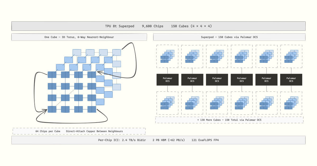
[ICI] links come straight out of the TPU die: high-speed [serial lanes], [direct-attach copper] inside a 64-chip cube (a 4×4×4 arrangement that lives in one liquid-cooled rack), optical between cubes. Per-chip aggregate [ICI] bandwidth has scaled from ~250 GB/s on [v2] to * 1.2 TB/s bidirectional on *, and
[Ironwood] that on
2×*. Topology alternates by generation:*
[v8t][2D torus]on the efficiency-tuned chips (

[v2],

[v3],

[v5e],

[v6e]),

[3D torus]on the flagships (

[v4],

[v5p],

[v7],

[v8t]).
The piece with no NVIDIA analogue is the : a
[Palomar OCS] that sits between cubes. Tiny mirrors physically rotate to map any input fibre to any output. A
[3D-MEMS][optical circuit switch][v4]

[superpod]uses 48 Palomar switches to wire 64 cubes (4,096 chips) into one 3D torus;

[v5p]and
[Ironwood]scale the same scheme up. Reconfiguration is millisecond-class, not nanosecond, but that's fine, because
[OCS]is : pick a topology at job start, run it for a week, then reconfigure for the next workload. Three problems collapse into one component: topology reconfiguration per workload (
**circuit-switched**[twisted tori]give up to 70% better

[bisection]), sub-pod

[slicing]on demand, and
(when a chip dies, the
fault tolerance[OCS]optically swaps in a spare cube and the run continues without losing the
[ICI]domain). This makes the the unit of scale-up: equivalent in role to NVIDIA's NVL72, two orders of magnitude bigger.
[superpod]

[v4]was 4,096 chips;

[v5p], 8,960;
is 9,216 chips arranged as 144 cubes of 64, presenting
[Ironwood (TPU v7)]*as one coherent*

**1.77 PB of**[HBM](~68 PB/s) and 42.5 ExaFLOPS[FP8][ICI]domain.
stretches this to
[TPU 8t (Sunfish)] .
**9,600 chips, 2 PB of**[HBM](~62 PB/s), and 121 ExaFLOPS FP4*has*

[TPU 8i (Zebrafish)]*. 8i replaces torus with a new hierarchical*

**1,024 chips, ~295 TB of**[HBM](8.8 PB/s), and ~10 ExaFLOPS FP4[high-radix]topology called

*(4-chip ring → 8-board group → up to 36 groups linked by*

[Boardfly][OCS]), cutting

[all-to-all]latency in half. This is designed for

[MoE]inference. A 3D torus excels when

[collectives]are nearest-neighbour (

[ring all-reduce]uses every link every cycle), but
[MoE expert routing]is the opposite pattern,
[all-to-all]: every chip ships unique fragments to every other, and round-trip latency is bounded by the longest-hop pair. A 1,024-chip 3D torus has a 16-hop diameter; [Boardfly]'s ring → group → OCS hierarchy compresses that to 7.
Scale-out
Through [TPU v7], scale-out ran over a single fabric: ,

[Jupiter]
via
all-optical at the spine since 2022*, the same 3D-MEMS family as*
[Apollo OCS][Palomar], scaled across the building. Google uses the same primitive (optical circuit switching) at every layer from rack to datacenter spine; that is the architectural signature nobody else has.
[Jupiter]today carries 13 Pb/s of

[bisection]per building.

With , scale-out split into two fabrics. East-west TPU-to-TPU traffic moved to

[TPU 8t]
, a dedicated accelerator fabric;
[Virgo][Jupiter]retained the role: storage access, general compute, and inter-site scaling.
north-south[Virgo]is a topology built on
[flat],[two-layer],[non-blocking]*switches: every TPU is at most two switches from any other. One*

[high-radix][Virgo]cluster links 134,000+

[TPU 8t]s at 47 Pb/s of

[bisection](4× the per-chip bandwidth and 40% lower

[unloaded latency]than the prior

[DCN]generation), with

[multi-planar fault isolation]and
[sub-millisecond telemetry]that lets the scheduler kill stragglers before they wreck a step. The architectural payoff is that each layer can now evolve independently: scale-up, east-west scale-out, and front-end can iterate on different cadences without rewiring the others.
Per-chip scale-out bandwidth is on the order of * 100 Gbps on *, and
[Ironwood] that on
4×*, but still two orders of magnitude less than per-chip*
[v8t][ICI]. This bandwidth gap dictates partitioning:

[tensor parallelism]and

[MoE expert routing]stay inside

[ICI];

[data parallelism]and

[pipeline parallelism]cross the scale-out fabric.
Google's framework, plumbed into
[Multislice] , lets a single
[XLA](https://openxla.org/xla)[SPMD]program span multiple

[slices]in different

[pods]; the compiler emits hierarchical

[collectives](

[ring all-reduce]inside each slice,

[higher-level reduce]across). The structure is exactly the trick for hiding the

[ICI]/
[DCN]bandwidth gap: as much work as possible stays inside the slice over fast ICI, leaving only the cross-slice residual to pay the slow-fabric cost.
Above this sits . Where
[Pathways]

[NCCL]+

[Slurm]+

[Megatron]-style

[schedulers]drive

[SPMD]from many controllers,

[Pathways]drives the entire job from
client and
**one**[virtualises]multiple "islands" (

[pods]with their own

[ICI]domains) connected over

[DCN]. It does

[gang scheduling],

[elastic training](when a slice fails,

[OCS]reshapes the topology and
[Pathways]resumes from the last checkpoint on the new shape), and
[cross-region orchestration]. was the first frontier model trained across multiple datacenters;
Gemini Ultra[Pathways]stitches them into one synchronous
[SPMD]job. The philosophy: * the compiler is the scheduler, the torus is the topology, and the optical switch is the universal reconfigurable substrate*, at every layer from rack to datacenter.
Software
The TPU stack is * compiler-driven* where CUDA is
. On a GPU, the developer writes the kernel and the
**kernel-driven**[framework]strings kernels together; the

[compiler]'s job is mostly
[local]. On a TPU, the developer writes a numerical program in
and
[JAX](https://github.com/jax-ml/jax)*is responsible for everything below it: which operations*

[XLA](https://openxla.org/xla)[fuse], where each tensor

[lives], how it is
[laid out]across the 2D vector registers, when
[DMAs]from

[HBM]to

[VMEM]issue, how the 322-bit

[VLIW]bundles are

[scheduled], how the program
[shards]across thousands of chips. There is no hardware fallback: no
[warp scheduler], no cache, no out-of-order engine to paper over a bad

[schedule]. The

[compiler]is the system. The trade-off is the central one of the architecture:
.
XLA gets closer to the theoretical[ceiling]without hand-tuning, but[closing the remaining gap]is harderThe compilation path is .
[JAX]→

[JAXpr]→

[StableHLO]→

[HLO]→

[LLO]→

[VLIW bundles]
traces a Python function into a
[JAX][typed]

[functional]

[IR](

[JAXpr]) under

[, lowers it to]
jit
(the
[StableHLO][OpenXLA]-standardised,

[versioned]

[op-set]of ~100

[statically-shaped primitives]that all

[front-ends]now

[emit]), which XLA

[ingests]as
and runs through its pass pipeline:
[HLO]*(collapse*

[operation fusion][pointwise]+

[reduction]+

[matmul]into one kernel so intermediates never hit HBM),
(decide the
[layout assignment][2D tiling]of every tensor so it

[streams]into the

[MXU]without a

[transpose]: substantially harder than on
[1D SIMD machines]because both the registers and the systolic inputs are 2D),
(every tensor pinned to either VMEM, CMEM, or HBM with
[buffer assignment][overlap windows]pre-computed), , and finally a VLIW
[SPMD partitioning][scheduler]that fills all eight slots of every bundle.

[HLO]lowers to

*(Low-Level Optimizer), the TPU-specific*

[LLO][IR], and LLO
[emits]the final VLIW stream. A well-compiled program overlaps
[MXU]systolic execution, VPU [element-wise math], and HBM↔VMEM DMA in the same bundle every cycle.
Multi-chip execution is : one program, sharded data, hierarchical
[SPMD]

[collectives],

[emitted]by
(now being replaced by
[GSPMD]*, an*

[Shardy][MLIR]-native successor that lands as the default in early 2026). The user expresses sharding

[declaratively]with
+
[Mesh]*annotations on a few key tensors; the*

[PartitionSpec][compiler]propagates shardings through the rest of the

[graph]and inserts

[all-reduces],

[all-gathers], and

[reduce-scatters]where the layout changes. When the

[compiler]picks a wrong collective,
drops the user into
[shard_map]*(per-device code with explicit local shapes and explicit*

**manual SPMD**[collectives]), composable inside
jit
so a single kernel can be hand-partitioned without giving up auto-partitioning everywhere else. This is the inverse of the PyTorch idiom: and
[FSDP]wrap the model in a runtime that issues
[DeepSpeed][collectives]at module boundaries; GSPMD/Shardy partitions the whole

[graph]as a

[compiler]problem.
is the escape hatch: JAX's kernel-writing language, broadly the TPU equivalent of
[Pallas] on GPUs. Pallas kernels are written in JAX-flavoured Python, lowered through
[Triton](the [Mosaic][MLIR]-based TPU backend) to LLO, and embedded back into HLO as a custom op. It exists because XLA cannot always synthesise the optimum for novel attention variants, fused MoE dispatch, or anything that demands manual VMEM tiling and DMA scheduling: a
optimisation, where the win is in the
FlashAttention-class[schedule]and not the algebra. targets H100/Blackwell with the same front-end, so a kernel author can write once and lower to either substrate. The library tier above this is uniformly JAX-native:
**Pallas:Mosaic-GPU*** for modules,*

[Flax NNX]*for optimisers,*
[Optax]for asynchronous distributed checkpointing,
[Orbax]*for input pipelines,*

[Grain]*for post-training/RL,*
[Tunix]for quantisation. Google's reference training stacks (
[Qwix]*for LLMs including DeepSeek-V3-class MoE, and*

[MaxText]*for Flux, Wan 2.1) sit at the top, in pure JAX;*
[MaxDiffusion]sits beneath, exposed to the user as
[Pathways], so a single Python client can drive a job across thousands of chips and several pod-islands without giving up the JAX programming model.
[pathwaysutils]The PyTorch path is real but second-class. uses a
[torch_xla] mechanism: every PyTorch op records into an HLO
[LazyTensor][graph]that compiles on the next barrier, with the compiled artifact cached by graph-shape hash. PyTorch/XLA 2.x added
,
GSPMD-style sharding annotations* through an XLA backend, a*
torch.compile
integration*, and (PyTorch/XLA 2.7) C++11-ABI builds with materially faster tracing. The gap to JAX is real (JAX's primitives map more cleanly to*
JAX bridge[StableHLO], and complex parallelism strategies are better-covered), which is why
(powered by the
[vLLM TPU]*plugin announced at Cloud Next 2025) lowers*

[tpu-inference]*model, JAX-defined or PyTorch-defined, through a*
every*.*
unified JAX→XLA path*, announced April 2026, is Google's response: a native PyTorch experience with eager mode,*
[TorchTPU]torch.distributed
, and torch.compile
over XLA, on track to replace torch_xla.Compared to CUDA, the TPU ecosystem is * centralised, not sprawling*. Almost everything below the framework (XLA, JAX, Flax, Optax, Pallas, MaxText, Pathways, Shardy, Mosaic) is open-sourced by Google itself, evolving in lockstep with the silicon. There are far fewer third-party kernels than CUDA's decades of accumulation; the moat is thinner where the workload looks weird, deeper where the workload looks like Gemini. The recent
language is the explicit framing: chip, ICI fabric, OCS, XLA, Pathways, Pallas, MaxText, vLLM, and Pathways co-released as one product, with v8t/v8i continuing the same model under a single tpu-inference lowering path.
Ironwood (v7) "codesigned AI stack"* and*
Triton* narrow the gap on the NVIDIA side (kernel-driven and compiler-driven are converging), but the philosophical poles are still real:*
torch.compile
on TPU the[compiler]is the only interface that matters; on GPU the[compiler]is one of several.### AMD GPU
The are built on a different bet from NVIDIA: where NVIDIA each generation expands what each SM can
AMD InstinctGPUs do, AMD has held the
conservative since
[Compute Unit][GCN](2012) and reinvested into the package: matched or beat the contemporary NVIDIA flagship on

[HBM]capacity every generation since 2021; the first

*datacenter GPU (CDNA 3); the first coherent*

**3D-stacked***(*

**CPU+GPU**[APU][MI300A]); and an
(
**open ecosystem**[ROCm],

[HIP], OCP MX,

[UALink]).
Genealogy
[XCDs]hybrid-bonded onto

[IODs]via

[TSV];

[FP8];

[Infinity Cache]; coherent CPU+GPU

[APU]on MI300A; powered

[El Capitan].
Architecture
| AMD | NVIDIA |
|---|---|
| Compute Unit (CU) | Streaming Multiprocessor (SM) |
| SIMD | SM Sub-Partition |
| SIMD Lane | CUDA Core (FP32 ALU) |
| Wavefront (wave64) | Warp (warp32) |
| Matrix Core | Tensor Core | | MFMA | mma.sync / wgmma / tcgen05.mma | | VGPR / SGPR | Register File | | LDS (Local Data Share) | SMEM (Shared Memory) | | Infinity Fabric | NVLink |
Where NVIDIA's architectural ambition lives inside each SM (new tensor primitives, new async machinery, new operand stores each generation), AMD's lives between the [CUs], in how many of them can be bonded into a single coherent package. The CU itself is conservative: four 16-lane [SIMDs], one shared scalar unit, a 64 KB [Local Data Share], an L1 vector cache, a per-SIMD [VGPR] file with a CU-shared [SGPR] pool, and (since CDNA 1) a [Matrix Core] running [MFMA]. The shape hasn't meaningfully changed since [GCN] in 2012; what scales is the count (120 CUs on [MI100], 220 on [MI250X], 304 on [MI300X], 256 on [MI355X]) and the packaging that bonds them. A [wavefront] of 64 threads streams across the 16 SIMD lanes over 4 cycles, with many wavefronts resident per SIMD that the scheduler switches between to hide stalls. There's nothing exotic in here; what's interesting about CDNA is everything outside the CU.
Compute
Inside the CU, the SIMDs and the Matrix Core run side by side. The four [SIMDs] handle everything element-wise: activations, normalization, residuals, address arithmetic. The [Matrix Core] handles the matmul. The split is the same as NVIDIA's [CUDA Cores] / [Tensor Cores] split, but the matrix abstraction has evolved on a very different curve.
NVIDIA's Tensor Core climbed the thread hierarchy: a 32-thread [warp] on [Volta], a 128-thread [warp-group] on [Hopper], a single thread plus an optional [two-SM cluster] on [Blackwell]. AMD's Matrix Core stayed put. Every generation of [MFMA] (from MI100 in 2020 through MI355X in 2025) is wavefront-scoped: one [wave64] issues a single matrix op (V_MFMA_*
), the four SIMDs cooperate to drive it, and operands come from the wavefront's register file: A and B from [VGPRs], C and D usually from the dedicated [AGPR] file. The instruction got faster and the format set widened, but the issuer and the scope did not. The one feeder-side concession came with CDNA 4: a dedicated MFMA transpose-load from LDS that hands operands to the Matrix Core already in the layout it wants, small in spirit to NVIDIA's TMA, but the matrix op itself stayed wave-issued.
The throughput numbers tell the format story directly. CDNA 1 launched in 2020 with FP32 / FP16 / [BF16] / INT8 at 256 / 1024 / 512 / 1024 FLOPs per CU per cycle, with native [BF16] support alongside [A100]. CDNA 2 doubled the [FP64] path to a full-rate matrix at 256 FLOPs/CU/cycle: uniquely AMD, the bet that put MI250X into [Frontier]. CDNA 3 reached parity with [H100] on [FP8] at 4,096 FLOPs (E4M3 + E5M2), added 2:4 [structured sparsity], and added a [TF32]-equivalent path that runs FP32 matmul at the FP64-matrix rate by truncating mantissas. CDNA 4 doubled again to [FP4] at 16,384 FLOPs and FP6 with [OCP MX block-scaling], and added mixable A/B precision in one MFMA: FP8 × FP4, for example. The same generation halved per-CU FP64 throughput, the first AMD chip to trade HPC density for AI density rather than ship both.
The wavefront-scope decision shows up in two costs.
-
Divergence.* A half-empty [wave64]wastes 32 lanes where a half-empty warp32 wastes 16. For workloads with mostly-uniform control flow this is a small price; for irregular workloads it hurts.
-
Overlap.* NVIDIA's asynchronous, descriptor-driven matmul decouples issue from execution: the issuing thread fires the instruction and moves on; the Tensor Core runs in the background; the warp can run softmax, apply a mask, or pre-load the next tile while the previous matmul is still in flight. AMD's wavefront-collective MFMA gives the wave no equivalent: the same wave that issued the matmul can't simultaneously do meaningful vector work while it's pending. Overlap is possible across separatewavefronts, but has to be staged in software with explicit wavefront barriers, which is more fragile and consumes more wave slots and registers.
How much this matters depends on the workload. * Pure dense GEMM* (DGEMM, the inner loop of large-batch training) has nothing useful to do during the matmul; both engines saturate; async buys little. These are exactly the workloads where AMD has historically led at exascale HPC (
[Frontier]on MI250X,

[El Capitan]on MI300A).
(
Transformer attention[FlashAttention-3], FA4) interleaves matmul with softmax, masking, and KV-cache reads, and the async overlap is the whole structure of those kernels. AMD has to recreate the pipeline by hand, which lags NVIDIA's hardware-level support.
sit in the same camp: address-irregular work that wants to run alongside the matmul.
MoE dispatch, paged attention, speculative decode NVIDIA's matrix-instruction abstraction has moved further across generations (warp → warp-group → single-thread async + cluster), and AMD hasn't followed.
Memory
AMD's memory hierarchy has fewer general-purpose tiers than NVIDIA's, with one giant cache that NVIDIA does not have at all. From the CU outward: a 64 KB [LDS] scratchpad (software-managed, 32-bank, AMD's analog of NVIDIA's [SMEM]), a vector L1 (16 KB on early CDNA, 32 KB from [MI300X] onward), a per-[XCD] L2 of a few MB. The L2 isn't coherent across XCDs, though; coherence happens one tier above L2.
That tier is the [Infinity Cache]: 256 MB on MI300X, distributed across the four [IODs], 16-way set-associative, ~12 TB/s measured, more than twice MI300X's 5.3 TB/s of [HBM3]. It originated on RDNA gaming GPUs to compensate for narrow GDDR buses; AMD reused the IP for AI on CDNA 3, where attention KV reuse and weight reuse fit a large LLC unusually well. NVIDIA bet on bigger HBM bandwidth instead (8 TB/s on [B200], scaling with [HBM4] on [Rubin]), and AMD bet on the cache.
Off-chip, the HBM capacity grows aggressively: 32 → 64 → 128 → 192 → 256 → 288 GB across [MI100] / [MI210] / [MI250X] / [MI300X] / [MI325X] / [MI350X], matching or exceeding the contemporary NVIDIA flagship in every generation from 2021 onward. The bet is that inference workloads are increasingly capacity-bound, and that the chip with more memory wins.
Numerics
The format trajectory tracks the precision-halving pattern that everyone in AI silicon shares: FP32 → FP16 → FP8 → FP4, restoring accuracy each step with finer-grained scaling. The AMD-specific axis is * openness*. CDNA 4's
[FP4]and FP6 use : the same numeric format as
[OCP MX]block-scale multiplication[Blackwell]'s MXFP4 and TPU v8's MXU, but specified by an open consortium (AMD, NVIDIA, Intel, Meta, Microsoft, Qualcomm, ARM) that AMD helped found, rather than by any single vendor. The format that ships in MI355X is identical to what ships in B200 and TPU v8.
The CDNA 4 inflection deserves its own line: per-CU FP64 throughput halved. [MI300X] served training, HPC, and inference together; [MI355X] is an AI chip first. The full-rate FP64-matrix bet that powered [Frontier] hasn't been killed, but it's no longer carrying the weight.
Chiplets
The packaging is where CDNA stops looking like NVIDIA and starts being something else.
CDNA 1's [MI100] was monolithic 7 nm. CDNA 2's [MI250X] was AMD's first multi-chip GPU: two [Aldebaran] GCDs side-by-side on a 2.5D EFB organic substrate, joined by 4 in-package [Infinity Fabric] links at 400 GB/s aggregate, but presented to software as two separate GPUs.
CDNA 3 is the move that changed everything. Eight (TSMC N5, ~115 mm² each) are stacked in 3D via
[XCDs]

*hybrid bonding (sub-micron-pitch*

[TSMC SoIC]*, no microbumps) onto four*

[TSVs]*(TSMC N6) below. The IODs carry the*

[I/O dies][Infinity Cache], the
[HBM3]PHYs, the Infinity Fabric links, and
[PCIe Gen 5]; each IOD hosts two XCDs above and two HBM stacks beside. The four IODs are stitched by
at 4.8 TB/s bisection, so the 153-billion-transistor package looks like one GPU to the kernel: cache and address space unified at the IOD layer. NVIDIA stayed monolithic through
[Infinity Fabric AP][H100]and only went to two reticle-limit dies on

[B200]via 2.5D
[CoWoS-L]. AMD got to 3D stacking a generation earlier, at smaller per-die area: different bets on the same packaging frontier.
The pushed the bet further. Replace 2 of the 8 XCDs with three Zen 4
[MI300A]

[APU]
, leave HBM and Infinity Cache and the IODs intact, and let CPU and GPU share one physical address space backed by HBM3 with hardware coherence. There is no host-device copy. There is no pinned memory. There is no PCIe in the path. Zen 4 cores and CDNA 3 XCDs read from the same pages. NVIDIA's
[CCDs][Grace-Hopper]bridges twopackages over
[NVLink-C2C]; MI300A is one.
(11,039 nodes of 4× MI300A) is the deployment that justified it.
[El Capitan]On CDNA 4's [MI355X], eight [XCDs] are still 3D-stacked via [SoIC] onto base dies below, but the XCDs move to TSMC N3P with 32 active CUs apiece (256 total, vs 304 on [MI300X]; the per-XCD count dropped to free area for bigger [Matrix Cores] and a 160 KB [LDS]). The four MI300X [IODs] collapse to two, each twice as wide on TSMC N6, hosting four XCDs above and four [HBM3E] stacks beside. Each IOD now carries its own 128 MB slice of the 256 MB [Infinity Cache], half the HBM PHYs, its share of the [Infinity Fabric] links, and [PCIe Gen 5]. [Infinity Fabric AP] between the two IODs runs at 5.5 TB/s bisection (~15% above CDNA 3), and the eight stacks shift to 12-Hi HBM3E for 288 GB at 8 TB/s, 50% more capacity than MI300X on the same pin count. The package totals 185 billion transistors and still presents as one GPU to the kernel.
Bets
HPC and AI are the same betBet 1: HPC then AI.* until they aren't*: ship full-rate FP64 matrix from CDNA 2 through CDNA 3, then bifurcate at CDNA 4 once inference economics decisively favour low precision.Match or beat the contemporary NVIDIA flagship on HBM capacity every generation since 2021, and add a 256 MB last-levelBet 2: Memory capacity.[Infinity Cache]that absorbs the reuse H100 must hit HBM for.3D-stack compute on cache and I/O before NVIDIA does: TSMC** Bet 3: Early 3D-stacking.[SoIC]hybrid-bonded XCDs on IODs in 2023, while NVIDIA stayed monolithic until 2025.The Bet 4: Coherent CPU+GPU.[MI300A]APU is the most chiplet-aggressive product ever shipped, and the[El Capitan]deployment is the proof. Bet 5: Open scale-up fabric.**[UALink]and OCP MX over[NVLink]and proprietary FP4.
Scaling
The memory bet has a scaling consequence: when 8 [MI300X] chips hold 1.5 TB of HBM and 8 [MI350X] chips hold 2.3 TB, you can fit a 405B-parameter model in [FP8] inside a single 8-GPU box (weights, KV cache, and headroom for longer contexts and bigger batches), where the same model on 8× [H100] (640 GB) requires careful sharding. For inference workloads through 2024–2025, AMD's scale-up didn't need to match NVL72 at the rack to be competitive at the box. For training at the frontier, it did, and AMD didn't have an answer until 2026.
[InfiniBand].

[Pensando]NICs (

[Pollara 400],

[Vulcano 800]) implement the

[Ultra Ethernet Consortium]'s

[UET]

[RDMA]transport;

[Broadcom Tomahawk 6]supplies the

[switch ASIC]and

[CPO].
Scale-up
Through MI355X, AMD's scale-up means an 8-GPU OAM platform over
[Infinity Fabric]. Each [MI300X]has 7 IF links (one to every peer in the box) at 128 GB/s bidirectional, giving 896 GB/s of per-GPU mesh bandwidth in a fully-connected all-to-all topology.
[MI350X]bumps each link to 153.6 GB/s (~1,075 GB/s per GPU) but keeps the 8-GPU shape. The platform conforms to OCP's UBB 2.0: the same mechanical socket as an NVIDIA HGX baseboard, so server vendors can ship AMD or NVIDIA on the same chassis without redesigning the system.
What AMD didn't ship through MI355X was a rack-scale equivalent of NVL72. Customers running larger models on MI300X clusters scaled across multiple 8-GPU boxes via Ethernet, paying scale-out latency for what NVIDIA users could keep inside scale-up. This was the gap that mattered for training, and the gap that is built to close.
[Helios] Helios is AMD's first rack-scale scale-up domain, shipping in 2H 2026 alongside [MI455X]. 72 GPUs per rack, ~31 TB [HBM4], 1.4 PB/s aggregate HBM bandwidth, 2.9 ExaFLOPS FP4 / 1.4 ExaFLOPS FP8, 260 TB/s of scale-up bandwidth, 43 TB/s of scale-out. The form factor is ** Open Rack Wide (ORW)** (Meta's 2025 OCP submission, double-wide and liquid-cooled), not an AMD-proprietary chassis. Building on Meta's reference design rather than designing a rack from scratch is a deliberate AMD bet: any hyperscaler standardised on ORW can deploy Helios without bespoke datacenter facilities work.
The fabric is : Ultra Accelerator Link, an open consortium standard AMD helped found alongside Apple, AWS, Cisco, Google, HPE, Intel, Meta, Microsoft, and Synopsys. UALink 200G 1.0 (April 2025) defines a 200 GT/s lane and 800 Gbps per direction, with switched topologies scaling to 1,024 accelerators per pod. The promise is a cache-coherent interconnect comparable to NVLink but unowned: any vendor can build a UALink switch, any accelerator can talk UALink, the standard belongs to the consortium rather than to the strongest seller.
[UALink] The catch: native UALink switching silicon won't ship in volume until 2027. Astera Labs' Scorpio, plus competing parts from Auradine, Enfabrica, and Xconn, are all targeting late-2026 / 2027 deployment. Helios at launch uses (Infinity Fabric tunnelled over standard Ethernet) as a stopgap, preserving the programming model while waiting for native UALink fabric. Native UALink switching arrives with MI500 in 2027. At launch, Helios is closer to a fast Ethernet-tunnelled coherent cluster than to NVL72's true cache-coherent NVLink domain: a real concession on the timeline, paid in exchange for hitting 2H 2026 with a competitive product.
[UALoE]
Scale-out
AMD does not ship [InfiniBand]. The whole scale-out stack is Ethernet, anchored on a different open standard: the .
[Ultra Ethernet Consortium (UEC)] UEC 1.0 (released June 2025) defines : a new RDMA transport over standard Ethernet, with packet spraying, SACK-based selective retransmit, and modern congestion control. UET is not RoCEv2 (which encapsulates InfiniBand transport in Ethernet frames); it's a clean redesign of RDMA semantics for scale-out AI fabrics. AMD is a founding member alongside Broadcom, Cisco, Meta, and Microsoft. Same play as UALink: own the standard, not the implementation.
[Ultra Ethernet Transport (UET)] The NIC is , the networking startup AMD acquired in 2022.
[Pensando] is the current AI NIC: 400 GbE, P4-programmable, UEC-ready, PCIe Gen 5, paired with MI300X / MI355X.
[Pollara 400]ships in 2026 alongside MI455X: UEC 1.0 compliant, PCIe Gen 6, native UALink interfaces, 8× the per-GPU scale-out bandwidth of Pollara.
[Vulcano 800]is the front-end DPU (16× Arm Neoverse-N1, dual 400 GbE) for storage / SDN / firewall, equivalent to NVIDIA's
[Salina 400][BlueField], distinct from the AI back-end NIC. The switch silicon, though, isn't AMD's. Helios's 43 TB/s scale-out fabric runs through : a 102.4 Tbps Ethernet switch ASIC with co-packaged optics ("Davisson"). AMD has no in-house
[Broadcom Tomahawk 6] [CPO]and no in-house switch ASIC; the optical layer is partner silicon. NVIDIA owns its entire stack: InfiniBand, Spectrum-X Ethernet, ConnectX, BlueField, Quantum-X Photonics CPO, all in-house. AMD owns one tier (NIC + DPU via Pensando) and bets that open standards plus best-of-breed partner silicon will outpace vertical integration.
The industry has moved AMD's way. Dell'Oro reports Ethernet handled more than twice the AI scale-out fabric volume of InfiniBand in 2025; AWS, Microsoft, Meta, Oracle, and xAI have all standardised on Ethernet for their AMD-based AI clusters. The remaining question isn't whether Ethernet can match InfiniBand on RDMA semantics (UEC closes that gap) but whether Helios can close the rack-scale gap with NVL72 fast enough to win frontier training workloads that today default to NVIDIA.
Software
is the open-source counterpoint to
ROCm . Where NVIDIA's stack is proprietary and vertically integrated (cuBLAS, cuDNN, TensorRT-LLM ship as binary blobs maintained by NVIDIA alone), ROCm is GitHub-native and bets on open standards (PyTorch, Triton, vLLM, OCP MX) rather than a walled-garden library set. The software gap with NVIDIA is real, but AMD's strategy is to close it through the open community rather than build a parallel CUDA stack from scratch.
[CUDA](https://docs.nvidia.com/cuda/cuda-c-programming-guide/)The bottom of the stack is , AMD's CUDA-compatible C++ runtime.

[HIP]
translates CUDA source to HIP automatically. Bulk HPC code (HACC, Laghos, QMCPack) ports at 80–95% out of the box: the CORAL-2 number. Modern AI kernels port worse: anything that reaches for Hopper- or Blackwell-specific primitives (
[hipify][TMA]descriptors,

[,]
wgmma
tcgen05.mma
) has no clean ROCm analog and has to be rewritten by hand.Above HIP sits a library tier structured to mirror NVIDIA's, one-to-one by name: for cuBLAS;
rocBLAS for cuBLASLt;
[hipBLASLt](https://github.com/ROCm/hipBLASLt)*for cuDNN;*

[MIOpen](https://github.com/ROCm/MIOpen)*for NCCL;*

[RCCL](https://github.com/ROCm/rccl)*(and its modern*

[Composable Kernel][ck-tile]DSL) for CUTLASS; rocprofv3 / rocprof-sys / rocprof-compute for the Nsight family. There is no first-party analog of TensorRT-LLM, though. AMD's answer is to back
as the open-source serving engine and ship AMD-specific operators (
vLLM) that plug into it; the dedicated ROCm CI for vLLM took test-pass rate from 37% to 93% across early 2026.
[AITER]The PyTorch path is first-class. Eager-mode PyTorch has run on ROCm since 2018; torch.compile
lowers through Triton, and Triton's ROCm backend (with [AOTriton] for ahead-of-time math kernels) is upstream. There is no XLA-style intermediate IR; ROCm compiles direct to HIP / Triton / CK. As Triton becomes the default kernel path in PyTorch, much of the porting cost evaporates: a kernel that runs through torch.compile
works on both CUDA and ROCm without source change. This is the architectural bet beneath AMD's open strategy: Triton's Python DSL becomes the cross-vendor lingua franca that sidesteps the need for a CUDA-equivalent kernel ecosystem.
is the load-bearing case.
[FlashAttention] is production on MI300X via Composable Kernel; PyTorch defaults to CK or AOTriton on ROCm.
FA2*(Hopper-tuned) is partially supported via AITER + CK, but Dao-AILab's canonical implementation remains CUDA-only.*
FA3*(Blackwell, March 2026) has no ROCm port at all.*
FA4*, Hazy Research's MI355X port of ThunderKittens (November 2025), claims forward-pass parity with hand-tuned AITER in ~500 lines. The pattern: open-source academic kernels close the AMD tail months after NVIDIA's, not years.*
HipKittensProduction deployment has validated the strategy. Microsoft Azure's * ND MI300X v5* instances went GA in May 2024; OpenAI runs GPT inference on them. Meta ships Llama 3 / Llama 4 inference on MI300X via the Grand Teton platform. Oracle OCI's
went GA in September 2024, with MI355X following in 2026. These are real serving fleets at hyperscaler scale, not pilots.
BM.GPU.MI300X.8 The honest gap is still real. Independent benchmarks (Phoronix, March 2026) put ROCm 7.2 at 10–25% slower than equivalent CUDA on standard PyTorch / vLLM / SGLang workloads, at equivalent precision on equivalent silicon. ROCm 7 reached feature parity but not perf parity. The FlashAttention-4 tail (research code that exploits Blackwell's newest primitives) is where NVIDIA's moat remains most durable; it has no clean ROCm analog and waits for a hand-written AITER kernel or HipKittens-class community port. NVIDIA ships engineers inside frontier labs; AMD ships kernels through GitHub. The strategies converge on common workloads (Llama inference, attention, dense transformer training) but the long tail of novel research code still costs MI300X / MI355X deployments engineering time NVIDIA users don't pay.
Cerebras WSE
builds the
Cerebras . The philosophy: the
largest chip ever shipped[memory wall]is a consequence of cutting the wafer. A fab prints dozens of dies onto 300 mm of silicon and saws them apart; the industry then spends its most exotic engineering (
[HBM],

[NVLink],
[CoWoS], 5,184 copper cables per rack) wiring the pieces back together at a small fraction of on-die bandwidth. Cerebras skips the saw. The
is one piece of silicon: 84
Wafer-Scale Engine[reticle fields], 46,225 mm², 900,000 dataflow cores, and every byte of on-chip memory in
[SRAM]one cycle from a compute unit.
Genealogy
Architecture
A GPU is a hierarchy: threads inside [warps] inside SMs, dies inside packages inside racks, each boundary with its own bandwidth, its own latency, its own programming construct; every accelerator built from dies inherits some version of it. The WSE is a * flat plane*: 900,000 identical cores tiled edge-to-edge in a 2D mesh, with no shared cache, no global memory, and no boundary of any kind between one core and the other 899,999. Each core is tiny, ~38,000 µm² on
[WSE-2], roughly half SRAM and half logic, peaking at 30 mW: 48 kB of local SRAM, sixteen general-purpose registers, a six-stage pipeline, a 4-wide FP16
[FMAC]SIMD (8-wide on

[WSE-3]), and a five-port router into the fabric. Execution is
: a core sits idle until a
[dataflow]arrives, control bits in the wavelet select which handler task fires, and eight hardware
[wavelet]switch cycle-by-cycle as tensor operands arrive and drain. No warps, no
[microthreads][warp schedulers], no caches to miss, no reorder buffer: the arrival of data is the schedule.
The Wafer
A stepper exposes a wafer one [reticle] at a time, ~850 mm² per shot, which is why every conventional chip lives under that ceiling (and why B200 became [two dies] the moment NVIDIA pressed against it). Cerebras prints the same ~550 mm² die 84 times in a 12×7 grid, like any other customer of TSMC, and then, in a process co-developed with TSMC, lays extra high-level metal across the <1 mm [scribe lines] where the saw would normally run. The mesh crosses each seam on a source-synchronous parallel interface (2,880 GB/s per die on WSE-3), and the entire inter-die layer costs ~97 W. To software the seams do not exist: one uniform mesh, one chip.
Wafer-scale has been tried before and it failed on yield: a single defect in a monolithic wafer-computer kills the whole wafer, which is what buried [the idea] in the 1980s. Cerebras's answer is granularity. A defect on an H100 disables an entire ~6 mm² SM; the same defect on a WSE disables one 0.05 mm² core. WSE-3 fabricates ~970,000 cores and ships 900,000: the ~7% spare pool, plus redundant fabric links, lets the hardware remap around every defect and restore a full logical mesh.
The Core
The unusual part of the core is not the datapath; it is what an instruction is. Alongside the sixteen general-purpose registers sit * 44 *, each holding a tensor descriptor:
[data-structure registers](DSRs)

[base address],

[extent], and
[stride], up to four dimensions. Instructions name their operands by DSR, so a single FMAC instruction says
multiply the arriving stream against this resident tensor and accumulate into that one, and the hardware streams elements for as long as the tensor lasts. There is no software loop around the multiply and no instruction fetch per element; the loop lives in the descriptor. NVIDIA spent five Tensor Core generations walking the matmul toward a single
[descriptor-driven command]; on a WSE core, a tensor instruction has no other form.
Sequencing is the fabric's job. A [color] is a statically routed virtual channel with a handler task bound to it at compile time, so sending a wavelet on a color is invoking code on the destination core: the 16 control bits are the call, the 16 data bits the argument. The * task scheduler* holds the in-flight tensor operations on the core's eight microthreads and switches among them every cycle by operand availability. It is the same stall-hiding job a
[warp scheduler]does with 64 resident warps, done with eight contexts, because the latency being hidden is a busy SRAM bank or a neighbour hop, not an HBM round trip.
The 48 kB of local SRAM is organised for the datapath rather than for locality: eight single-ported 6 kB banks deliver two 64-bit reads and one 64-bit write every cycle, exactly two 4-element FP16 operands in and one result out, the width of the WSE-2 FMAC. A 256-byte software-managed cache (512 B on WSE-3) keeps the hottest values beside the pipeline. This is the machine's thesis in miniature: per core, memory bandwidth and compute are matched exactly, and the wafer inherits that balance 900,000 times over.
Compute
There is no matrix unit on the wafer. NVIDIA, Google, and AMD all concentrate their FLOPs in a dedicated matmul engine ([Tensor Core], [MXU], [Matrix Core]) and differ mainly in how that engine is fed; Cerebras assembles matmul out of the fabric. A GEMM runs as a wafer-wide choreography: each arriving weight is broadcast along a row of cores holding activations, every core fires a multiply-accumulate against its resident slice (an [AXPY] per weight), and partial sums reduce across the mesh. The data reuse a Tensor Core gets from a register tile and an MXU gets from its wiring, the WSE gets from geometry: activations never move, so the only operand in flight is the one being multiplied.
The FLOPs ledger needs care, because the number Cerebras prints is not the number to compare. WSE-3's headline * 125 PFLOPS is sparse FP16*: it assumes the hardware's roughly 8× zero-skipping payoff on ideally sparse tensors. Dense is roughly
(derived: 900,000 cores × 8-wide FMAC × 1.1 GHz; Cerebras publishes no official dense figure). That is real compute, but it is not the point: per watt, dense FLOPs on the wafer lose to every contemporary GPU. The wafer was never a FLOPs machine. It is a
15.8 PFLOPS FP16*, and the FLOPs exist to keep up with the SRAM.*
bandwidth machine Zero-skipping is where dataflow earns its keep. Because computation is triggered by arriving data, a zero never triggers anything: * zeros are filtered at the sender*, and the receiving core never sees them and never spends the cycle. This is unstructured, element-granular sparsity, the general case that NVIDIA's 2:4
[structured sparsity]only samples. It is also, so far, an unexercised option. Cerebras's own sparse-pretraining results (
SPDF: 75% sparsity at 1.3B parameters; a follow-up at 6.7B) are vendor-authored and sub-7B, and no flagship customer model has been disclosed as sparse-trained: [Jais 2], the biggest run on the hardware, is dense. The only silicon that can harvest unstructured sparsity has yet to ship a headline model that uses it.
Memory
The hierarchy is one tier: * 44 GB of SRAM in 48 kB slices inside the cores, and nothing else on the wafer*. No HBM, no L2, no eviction policy; every byte is one cycle from an FMAC. The quoted bandwidth is 21 PB/s, and the number deserves its flag: it is the
sumof 900,000 local SRAM ports, an on-wafer aggregate, not a point-to-point link, and not comparable to an HBM figure. The honest comparison is bytes per FLOP: the wafer can feed ~1.3 bytes per dense FP16 FLOP, where a
[B200]gets ~0.002 from HBM. On that axis every GPU and TPU is starved; the WSE is the only machine in balance.
[Decode], the phase that is a pure bandwidth problem (one full read of the weights per token), is the phase the wafer turns out to be shaped for.
The other side of the tier is the edge of it. The wafer's connection to everything else is 12×100 GbE: * 1.2 Tb/s*, barely more than the single
[ConnectX-8]NIC attached to one Blackwell GPU. Between on-wafer SRAM and off-wafer Ethernet sit . NVIDIA's hierarchy descends gradually, each tier a few times slower than the last; the WSE has two tiers with a cliff between them. The wafer is an island, and the island's superpower and its cage are the same fact.
five orders of magnitude And the island is not growing. SRAM density has effectively stopped scaling on leading nodes: WSE-3 carries just 10% more SRAM than WSE-2 despite a full node shrink and a 54% jump in transistor count. Logic keeps shrinking; the six-transistor SRAM cell does not. The architecture's scarcest resource is the one thing the next process node no longer buys.
Weight Streaming
Training on the wafer inverts the flow everyone else takes for granted: on a GPU or TPU, weights are resident and activations stream through; on a WSE, * activations are resident and weights stream through*. Master weights live in
, a DRAM-and-flash appliance beside the cluster. Layer by layer, weights stream across the wafer, trigger multiply-accumulates against the activations pinned in SRAM, and leave; gradients stream back out on the backward pass, and the optimizer step runs inside MemoryX on CPUs (a weight update is O(parameters) of element-wise work with no reuse, so CPU-class compute keeps pace). The wafer never stores weights, "not even temporarily" (
[MemoryX]Cerebras's phrase). Model size is bounded by MemoryX, not by the 44 GB; the 44 GB bounds activations and batch.
What this buys is the programming model. One wafer holds a full layer's activations, so there is no [tensor parallelism], no [pipeline parallelism], no [FSDP] sharding: a 70B model is written as a single-device program, and multi-system scaling is * pure * through
[data parallelism] , a broadcast/reduce tree that fans one weight stream out to N wafers and sums their gradients on the way home. The parallelism-strategy spreadsheet that dominates GPU training simply has no Cerebras page.
[SwarmX]What it costs is scale, in the market's own revealed preference. The spec sheet says 2,048 CS-3s; the largest cluster ever disclosed is 64 ([Condor Galaxy 3]). The largest from-scratch model ever disclosed on the platform is * Jais 2 at 70B parameters and 2.6T tokens*, trained by anchor customer
[G42]with Cerebras engineers embedded. Nothing above 70B, from anyone, in the seven years since CS-1. And utilisation (
[MFU]), the number GPU labs publish as a matter of course at 35–45%, has never been disclosed for any Cerebras run.
Numerics
The numerics fit in a sentence: * FP16 and BF16 with FP32 accumulate*, plus (from WSE-3) a 16-wide 8-bit integer path that the Hot Chips disclosure labels fixed-point. No FP8, no FP4, no microscaling. While every other vendor halves precision each generation and buys the accuracy back with block scaling, Cerebras still computes in 16-bit and markets it as a quality differentiator ("the original 16-bit weights"). The tension is obvious: SRAM capacity is the architecture's scarcest resource, and 8-bit weights would halve the number of wafers a model needs. Whether 16-bit-only is numerical conviction or a datapath roadmap gap is an open question; no primary Cerebras source shows floating-point 8 anywhere on the wafer.
Bets
The die boundary is the tax the rest of the industry pays: SerDes, interposers, HBM stacks, cables, switches. Stitch 84 reticle fields in metal and the highest-bandwidth boundary in rival systems does not exist at all.Bet 1: Don't cut the wafer. Trade capacity for bandwidth at the steepest ratio in the industry: 44 GB at an on-wafer aggregate 21 PB/s. Balance the machine instead of hiding imbalance behind a hierarchy.Bet 2: SRAM is the only memory. 900,000 tiny cores triggered by arriving wavelets, with matmul assembled from broadcast, FMAC, and mesh reduction: skipping a zero is free rather than a special mode.Bet 3: Dataflow cores, no matrix unit. Weight streaming decouples model size (MemoryX) from wafer memory (44 GB) and collapses cluster scaling to pure data parallelism.Bet 4: Weights move, activations stay. The wafer re-reads an entire model per token faster than anything built on HBM; price that speed as a premium product instead of competing on cost per token.Bet 5: Sell latency, not throughput.
Scaling
Scale-up and scale-out mean something different here. NVIDIA's scale-up problem (make 72 packages behave like one device) is solved on the WSE by lithography: the coherent domain ships from the fab in one piece. What remains is everything past the wafer's edge, and no other machine hits its edge as hard or as early.
[colors], native broadcast, 214 Pbit/s aggregate fabric bandwidth. Fixed at 46,225 mm² by the size of a 300 mm wafer.
Scale-up
The wafer's internal fabric has no [SerDes], no cables, no transceivers, and no marginal cost per link: routing is compiled, each hop is one cycle, and a broadcast is a native fabric primitive rather than a switch feature. Where NVL72 spends 5,184 copper cables and a tray of [NVSwitch] ASICs to give 72 GPUs 130 TB/s of all-to-all, the WSE's equivalent domain is a single lithographic object. The catch is that the domain size is a constant. NVIDIA's scale-up domain grows every generation (NVL72 to NVL576 across three years); the wafer has been 46,225 mm² since 2019 and will stay there. 300 mm is the largest wafer the industry runs (the 450 mm transition died a decade ago), so Cerebras's scale-up roadmap is whatever the next node yields in density: there is no more area to be had.
Scale-out
Training scale-out is [SwarmX], and it only does one thing: replicate. Broadcast the weight stream to N wafers, reduce their gradients on the return path; batch grows with system count, model size does not. The claimed ceiling of 2,048 systems ("256 exaFLOPS", sparse) has never been built; 64 has.
Inference abandons weight streaming entirely; the arithmetic is fatal. Streaming a 70B model's 140 GB from MemoryX for every decoded token over a ~150 GB/s pipe would cost roughly a second per token. So inference * parks the weights in SRAM* and shards the model across wafers at layer boundaries: Llama 70B on "as few as four" CS-3s, pipeline-parallel over Ethernet, each additional wafer contributing 44 GB of weight-plus-
[KV]capacity and 23 kW of load. The speeds are real, and independently verified. measured 1,850 tokens/s on Llama 3.1 8B and 446 on 70B at the August 2024 launch, 969 on Llama 405B (240 ms to first token), and 2,522 on Llama 4 Maverick in 2025, ~2.4× the best published Blackwell number of the time. Vendor-quoted peaks run higher (2,100 on 70B with
[Artificial Analysis] [speculative decoding]; 3,000 on GPT-OSS-120B, where the live independent measurement sits nearer 2,000). No GPU provider comes close on per-user decode speed.
The economics are the sharp edge. Forty-four GB per wafer means a frontier-scale model consumes fleets: SemiAnalysis estimates ~24 CS-3s for a 1.6T-parameter-class model that fits in a handful of GPU racks, each system an analyst-estimated ~$450k bill of materials selling at a list price around $2–3M (never officially disclosed). During decode the wafer's enormous FLOPs mostly idle; Cerebras has declined to disclose batch sizes and has never published per-system throughput. Per-token API pricing runs roughly 3–5× GPU-based providers for the same open models, and Llama 405B was quietly dropped from the API, which SemiAnalysis reads as serving economics that didn't clear. Fixed SRAM also prices context: KV cache lives in the same 44 GB as weights, so long contexts steal capacity and force more systems per replica; the API caps at 131K tokens while frontier providers serve 256K–1M. [MoE] is served (Qwen3-235B at ~1,500 tokens/s, vendor-quoted) but is the format's worst case: a huge parameter footprint touched a few experts at a time, held in the most expensive memory.
The market has priced this honestly. Mistral's Le Chat (~1,100 tokens/s), Perplexity Sonar, and Meta's Llama API all pay for the latency; in January 2026 OpenAI signed for * 750 MW of CS-3 capacity through 2028*,
reported above $10Bat signing and since grown past $20B, the largest endorsement wafer-scale has ever received. The first flagship to ship on that capacity is
, launched July 2026 at a quoted 750 tokens/s.
GPT-5.6 Sol#### Software The stack is compiler-driven like the TPU's, but through a much narrower aperture: the Cerebras compiler is a * kernel matcher*, not a general code generator.
cerebras.pytorch
traces the training step through lazy tensors into Torch-MLIR and a graph IR, then matches subgraphs against a library of hand-written kernels, falling back to slower auto-generated ones for ops with no match. The documented constraintsare stark by GPU standards: static graphs only, no dynamic shapes, no data-dependent control flow, no eager tensor access mid-step, and a PyTorch version pinned behind upstream. The best independent practitioner account (
SURF, the Dutch national compute centre) reports unsupported layer types and no 1:1 porting path for standard PyTorch code.
And there is no kernel escape hatch. CUDA's answer to a novel attention variant is write a kernel; the TPU's is [Pallas]; ROCm's is [Triton]. The Cerebras ML stack has no user kernel path at all: when the matcher misses badly, the fix is a Cerebras engineer. A separate SDK language, , exposes the raw machine (tasks, wavelets, colors) and has produced striking HPC results (a
[CSL] TotalEnergies stencil codeat ~228× an A100, a Gordon Bell finalist on 48 CS-2s), but it is a separate world, unconnected to the PyTorch flow. Every flagship model on the platform (Jais, BTLM, Med42) was co-developed with embedded Cerebras staff.
There is a strange immunity in this. [FlashAttention], the defining kernel lineage of the GPU era, is a scheme for tiling attention through a memory hierarchy, and the WSE has no hierarchy to tile against: the optimisation class that costs AMD years of porting lag simply does not apply. But the immunity and the poverty are the same fact. The third-party kernel ecosystem that compounds on CUDA has no surface to attach to here; every kernel improvement in the platform's history has one author.
Where does that leave the wafer? Owning a real niche, honestly won: batch-one decode speed, independently verified, paid for by customers who price latency above cost. Around the niche, hard walls: 3–5× per-token pricing, a 70B training ceiling seven years in, revenue still ~86% concentrated in two Abu-Dhabi-linked customers in 2025 (per the S-1 filings around its May 2026 IPO), and a scarcest resource, SRAM density, that stopped scaling just as models kept growing. Hennessy and Patterson promised a Cambrian explosion; the WSE is its most extreme body plan, the one that decided the memory wall was a packaging choice and spent 46,225 mm² of silicon refusing to make it.
AWS Trainium
, the team behind AWS's
[Annapurna Labs] cards and
[Nitro]*CPUs, built*

[Graviton]*as a*
Trainium*. The compute core takes the TPU's proven playbook (a 128×128*
**fast-follower**[weight-stationary]

[systolic array], software-managed scratchpads, whole-program compilation) down to sharing Google's
compiler outright. The scale-out fabric is the
XLA-offloaded network that already carries the rest of AWS. What is genuinely Amazon's is narrow and deliberate: dedicated collective-communication silicon bolted onto the borrowed core, and the vertical integration to price a chip that only has to beat NVIDIA
[Nitro]inside AWS.
Genealogy
[FP8]acceleration, 96 GB

[HBM3]; the 64-chip

[UltraServer]. Powers

[Project Rainier].

[MXFP8/MXFP4]; the

[NeuronSwitch]all-to-all fabric replaces the torus. 144-chip UltraServer.
Architecture
The other captive-silicon story belongs to Google, and Trainium is best read as the TPU's thesis rebuilt inside a different cloud. The bets underneath are the same (a [systolic array] fed from software-managed [SRAM], scheduled ahead of time by a compiler, with no caches and no thread scheduler), but the unit is assembled differently. A Trainium chip carries a small number of * NeuronCores* (2 on
[Trn1], 8 on

[Trn2]and
[Trn3]), and each NeuronCore is not one monolithic matmul engine but a
: a
cluster of decoupled, specialised engines*(the 128×128 systolic array), a*
[Tensor Engine]for reductions, a [Vector Engine]for pointwise math, and a programmable
[Scalar Engine]of eight 512-bit vector processors for whatever fits none of the other three. Around them sit the data-movers: 128
[GPSIMD Engine]*, a*

[DMA engines]*that sequences transfers, and (from Trn2) dedicated*
Sync Engine* for collectives. There are no warps and no wavefronts; the engines run as a statically-scheduled dataflow pipeline, and the load-bearing design decisions are about what surrounds the systolic array, not the array itself.*
[CC-Cores]##### Compute The owns the matmul FLOPs; the other three engines own everything else. It is a 128×128 grid of processing elements (16,384
[Tensor Engine]

[MACs]) run

[weight-stationary]: one operand tile is loaded into the array and held in place (
LoadStationary
), the other streams through it (MultiplyMoving
), and partial sums land in , a small accumulator SRAM the engine can read-add-write so a contraction longer than 128 folds into place along the axis. This is the same tile
[PSUM][MMA]at the heart of every matmul accelerator; but where NVIDIA wraps it in the warp hierarchy and Google issues it from a
[VLIW]bundle, Trainium exposes it as a pair of explicit instructions against a named scratchpad.
The array is physically fixed at 128×128 across all three generations; what changes is how many products it packs per cell. [Trn1]'s NeuronCore-v2 ran [BF16]/FP16 with [FP32] accumulate and offered [FP8] only at the BF16 rate (no speedup). [Trn2]'s v3 double-pumps FP8 to present an effective 256×128 array, the first Trainium with a real 2× on 8-bit. [Trn3]'s v4 packs [microscaling] operands to present an effective 512×128 at 4× the BF16 rate. The count of physical multiply-add cells never moves; the datapath just feeds them narrower numbers.
The other three engines are what keep the array busy. The handles cross-element reductions (layernorm, softmax, pooling); the
[Vector Engine]

*handles one-in-one-out pointwise ops (activations, GELU); the*
[Scalar Engine], eight fully-programmable vector processors running C, absorbs anything that maps to none of them. A well-compiled step overlaps all four: the Tensor Engine grinds a matmul while the Vector Engine runs the previous tile's softmax and the DMA engines stage the next, the same producer/consumer overlap that makes TPU and GPU attention kernels efficient, expressed here as separate physical engines rather than separate warps or VLIW slots. The design pays off when a layer decomposes cleanly onto the four engine types, which transformers largely do. It pays a tax at the edges: an operator that fits none of the specialised engines falls to the programmable
[GPSIMD Engine][GPSIMD]path, slower, and the part of the machine most likely to bottleneck a novel architecture. It is Trainium's version of the long-tail cost every non-GPU accelerator carries.
Memory
The memory hierarchy is the compute philosophy applied to storage: * three tiers, all software-managed, no hardware cache anywhere*. AWS's own documentation draws the contrast, noting that unlike a CPU or GPU the NeuronCore has no cache and that "all memory movement is explicit in the program itself." Off-chip is
(32 GB on Trn1, 96 GB
[HBM][HBM3]on Trn2, 144 GB

[HBM3e]on Trn3). On-chip, closest to the engines, is the
: the main scratchpad, roughly 20× HBM bandwidth, organised in 128 partitions and sized per NeuronCore at 24 MiB (v2), 28 MiB (v3), 32 MiB (v4). Between the array and SBUF sits
[State Buffer (SBUF)], a 2 MiB accumulator dedicated to matmul outputs. Data moves HBM → SBUF → Tensor Engine → PSUM → SBUF, every hop issued by the compiler; nothing is prefetched or evicted by hardware.
[PSUM]This is exactly Google's [VMEM] bet, an explicit scratchpad the compiler must schedule perfectly with no cache to paper over a mistake, and the opposite of NVIDIA's hardware-managed [L2] and [L1]. Trainium inherits both the ceiling and the fragility that come with it: when the schedule is right the engines never stall, and when it is wrong there is no fallback path. The design runs a generous [HBM] budget against modest peak FLOPs, so per unit of compute Trainium carries more memory than a comparable NVIDIA part. On absolute capacity, though, it trails: Trn2's 96 GB sits below the [H200] and [B200], and Trn3's 144 GB (2025) sits below the 192 GB [B200] and 288 GB [B300] it ships against. So the lever AWS actually pulls when it argues the economics of serving a large model is not memory leadership but * price*: cost per unit of compute and HBM, on silicon it builds and rents itself.
Numerics
Trainium tracks the same precision-halving curve as everyone else (FP32 → BF16 → FP8 → FP4), with two Trainium-specific wrinkles. The first is : rather than fix
[configurable FP8]

[E4M3]and
[E5M2]like Hopper, the Tensor Engine takes an adjustable exponent bias and supports E5M2, E4M3, and E3M4, letting the compiler trade range for precision per tensor. The second is that
[Trn3]'s

[FP4]buys
no extra throughput: OCP
[MXFP4]operands are up-converted to MXFP8 before they reach the array, so FP4 runs at the FP8 rate and saves only memory and bandwidth, not compute. Both generations lean on the industry's accuracy-recovery tricks:
[microscaling]block exponents from Trn3, and hardware
on every generation. The one figure to distrust is the sparse peak: AWS headlines a 4× FP8 number that its own architecture pages put at 2× over dense FP8 (the 4× is relative to dense BF16), so the marketed acceleration and the datapath do not quite agree.
[stochastic rounding]##### Collectives in Silicon
The block with no clean analogue on a GPU is the . Distributed training and inference spend a large fraction of their wall-clock in
[collective-communication core]

[collectives]: every gradient step is an

[all-reduce], every

[MoE]layer an

[all-to-all]. On a GPU those collectives run as
[NCCL]kernels on the same SMs doing the math, so communication and compute contend for the same silicon and the overlap has to be won in software. Trainium carves the function out into dedicated hardware: 20
per Trn2 chip, wired straight to the
CC-Cores* ports, executing all-reduce, all-gather, reduce-scatter, and all-to-all while the Tensor and Vector engines keep running. It is the same move Google made with*
[NeuronLink][SparseCore]and Cerebras made with its off-core zero filter: find a workload the main engine is the wrong shape for, and spend a little area on a purpose-built block beside it rather than steal cycles from the core. Communication becomes something the chip does
concurrently, not something it s to do.
Bets
Annapurna designs chip, server, rack,Bet 1: The cloud is the product, the chip is a component.[Nitro]network, and cloud API as one stack, so Trainium only has to win on price-performance inside AWS, never on a merchant-silicon spec sheet.A 128×128Bet 2: Borrow the compute thesis, don't reinvent it.[weight-stationary]array, software-managed[SBUF]/[PSUM]scratchpads, and whole-program compilation are the TPU's bets, reused down to sharing Google's[OpenXLA]. The effort saved goes into the network and the rack.DedicatedBet 3: Collectives belong in silicon.[CC-Cores]overlap[all-reduce]and[all-to-all]with compute in hardware, instead of running them as kernels that steal FLOPs from the matmul units.Scale-out isBet 4: Reuse the cloud's own network.[EFA]with the[SRD]transport: the same[Nitro]-offloaded, packet-sprayed[RDMA]that already runs the rest of AWS. No[InfiniBand].Trn1 and Trn2 copied the TPU'sBet 5: Move the topology to the workload.[torus]; Trn3's[NeuronSwitch]replaces it with a switched[all-to-all]fabric as[MoE]traffic outgrew nearest-neighbour. Honestly, this is following the playbook: first Google's, now NVIDIA's.
Scaling
Trainium's scaling inherits its split from the rest of AWS: a tightly-coupled domain for the chips that must act as one, and the cloud's general-purpose
[NeuronLink] fabric for everything beyond it. The scale-up domain is not cache-coherent shared memory the way
[EFA][NVLink]is; AWS markets the [UltraServer]as a pooled multi-terabyte memory, but underneath it is message-passing over point-to-point links, closer in spirit to the TPU's
[ICI]than to an

[NVSwitch]crossbar.

[NeuronLink]binds chips into one
[UltraServer]. Through Trn2 the topology is a
[torus](16 chips per instance in a 4×4 2D torus, 64 per UltraServer in a 4×4×4 3D torus); Trn3 replaces it with the
[NeuronSwitch]all-to-all fabric. Message-passing, not coherent load/store. [Elastic Fabric Adapter]over Ethernet, offloaded to
[Nitro]. The

[SRD]transport sprays each flow across many paths and delivers reliably but out-of-order;
[UltraClusters]reach hundreds of thousands of chips over the
[10p10u]fabric.
Scale-up
NeuronLink is Trainium's chip-to-chip fabric, the role [NVLink] plays for NVIDIA and [ICI] for the TPU. Through Trn2 it wires chips into a , exactly the TPU's choice: a single
[torus] instance is 16 chips in a 4×4 2D torus at ~1.28 TB/s per chip, and the
[trn2]joins four instances into 64 chips on a 4×4×4 3D torus, presenting 83 dense
[Trn2 UltraServer][FP8]PetaFLOPS and ~6 TB of [HBM]as one scale-up domain. The third torus axis is deliberately thin (the inter-instance ring runs at ~256 GB/s per chip against 1.28 TB/s inside an instance), which is the torus's characteristic trade: cheap wiring and huge nearest-neighbour bandwidth, at the cost of many hops across the diameter. AWS positions the 64-chip UltraServer against NVIDIA's 72-GPU
[NVL72]; the aggregate compute is in the same league, but a torus is not a
[crossbar], and the two behave very differently on traffic that is not nearest-neighbour.
That trade is why Trn3 abandons the torus. is a switched
[NeuronSwitch-v1] fabric that roughly doubles inter-chip bandwidth and, more importantly, flattens the diameter so any chip reaches any other in one switched hop. The Trn3 UltraServer scales to 144 chips for 362 dense FP8 PetaFLOPS and 20.7 TB of
[all-to-all][HBM3e]. The motivation is the one that also pushed Google toward high-radix topologies for

[MoE]inference:
[expert routing]is all-to-all, the worst case for a torus, and a switch turns the longest-hop pair into a single crossing. Trainium's interconnect roadmap is a compressed re-run of the industry's: adopt the torus while the workload is nearest-neighbour, switch to a crossbar when it is not.
Scale-out
Scale-out is not bespoke; it is the same fabric AWS already runs. Every Trainium instance carries an [Elastic Fabric Adapter][NIC] into the datacenter network (3.2 Tbps per Trn2 instance), and the transport is , offloaded to the
[SRD (Scalable Reliable Datagram)] cards rather than run on the accelerator. SRD is AWS's clean-sheet answer to
[Nitro][RDMA]: instead of the single ordered flow of

[RoCE]or
[InfiniBand], it sprays each message across up to 64 parallel paths and delivers reliably but out-of-order, pushing reassembly up to the collective library and sidestepping the head-of-line blocking a single congested path would cause. It is the transport AWS built for its cloud generally, repurposed for the accelerator fabric.
At the top of the hierarchy is the , stitched together by the
[UltraCluster] network (AWS's shorthand for ~10 petabits/s of bandwidth at under 10 microseconds of latency across a datacenter) and scaling to hundreds of thousands of chips. The proof point is
[10p10u]: roughly half a million Trainium2 chips across multiple US datacenters, brought online for
[Project Rainier]Anthropic in late 2025; by early 2026 Claude was running on over a million chips, the largest commitment any external lab has made to a non-NVIDIA training platform. It exists because the economics close end to end. AWS claims Trainium2 delivers 30–40% better price-performance than its
[Hopper]-class GPU instances (an AWS figure, measured against last-generation NVIDIA rather than

[Blackwell]), and because Amazon owns every layer from the
[Nitro]card to the API, that margin is Amazon's to set.
Software
Trainium's software makes the borrowing explicit: the is a
Neuron SDK . The Neuron compiler (
compiler-first stack built on the same[OpenXLA]foundation as the TPUneuronx-cc
) ingests [XLA HLO]graphs and lowers them to a binary that the Neuron runtime loads onto the NeuronCores; the front-end IR is Google's, and Google's own OpenXLA announcements list Trainium as a first-class
[NEFF][PJRT]device alongside the TPU. runs PyTorch through
[torch-neuronx][PyTorch/XLA]'s

[LazyTensor]tracing (record ops, compile the graph at a step boundary), and
lowers JAX through
**jax-neuronx**[StableHLO]. On the spectrum from kernel-driven

[CUDA]at one pole to whole-program
[XLA]at the other, Trainium sits almost on top of the TPU: the compiler is the system, and it is largely the same compiler.
Where it diverges is the escape hatch. XLA alone cannot always synthesise the optimum for a novel attention variant or a fused MoE dispatch, so Neuron ships , a Python, tile-level kernel language that exposes the four engines and the
[NKI (Neuron Kernel Interface)]

[SBUF]/
[PSUM]scratchpads directly. It is Trainium's
(or its
[Pallas]): the same idea of a tile DSL that drops beneath the whole-program compiler when a kernel's win is in the
[Triton][schedule], not the algebra. Below it, a maps
**collective-communication library**[all-reduce]and

[all-to-all]onto the

[CC-Cores]and the NeuronLink topology (the

[NCCL]analogue), and
provides the sharded-training layer.
[NeuronX Distributed]The gap to CUDA (and even to the TPU's stack) is maturity, not design. NKI, the JAX path, and the distributed library were all still in beta through late 2024; a ported model runs only on AWS, with no cross-vendor fallback; and the [vLLM] backend trails the upstream project. The clearest tell is how the anchor tenant works: Anthropic does not simply target Trainium through PyTorch, it embeds with Annapurna, writes its own low-level [NKI] kernels, and upstreams fixes into the Neuron stack. Trainium is production-viable at the frontier, but at the frontier it is co-engineered, not turnkey: the compiler is inherited and excellent, but the surrounding ecosystem is young.
Groq LPU
The is a
GroqLPU machine. Every other chip spends silicon tolerating uncertainty: caches to hide memory latency, schedulers to fill stalls, arbiters to resolve contention it cannot predict. The LPU deletes all of it. Strip out every
deterministic* component (no cache, no branch predictor, no arbiter, no reorder buffer, not even an on-chip crossbar) and hand the entire scheduling problem to the compiler, which places every instruction and every byte on an exact cycle. What is left is a chip whose latency is known before it runs. Where the*
reactive* moved scheduling into the compiler but kept*
[TPU][HBM]and a dynamic network, Groq removed the last sources of nondeterminism: memory is all [SRAM], and the network is scheduled too, so hundreds of chips run as one clock-exact program.
Genealogy
[Jonathan Ross], who started Google's [TPU]as a 20% project, leaves to build a deterministic inference chip.
[ISCA]2022: [software-scheduled networking]extends the deterministic schedule across thousands of chips via a compiled
[Dragonfly].

[SF4X]; it never shipped (a reported failed tapeout).
[Language Processing Unit]; the company pivots from selling cards to selling tokens, on record decode speeds.
[non-exclusive license]to the LPU technology and hires Ross and much of the team.
[GTC]2026 as a latency co-processor beside

[Rubin]NVL72, via

[Attention-FFN disaggregation].
Architecture
The rest of the field is built from a * replicated core*: tile one
[SM],

[TensorCore],
[CU], or dataflow core across the die and farm work out to the copies. The LPU is built the other way. It takes a single conventional core and
: instruction control, the vector ALUs, the matrix units, the memory, and the network each become a
pulls it apart*, a full-height column of identical hardware, and the columns stand side by side across the die. Homogeneous down each slice, heterogeneous across the chip. Data does not sit in a register file waiting to be issued onto a unit; it*
[functional slice]horizontally through the slices like parts down an assembly line, East and West, one register hop per cycle, while
[streams][VLIW]instructions issue Northward from the control slices to meet it. Nothing in the datapath reacts: the compiler knows where every operand is on every cycle, and the hardware just turns the clock. The streaming is the identity: this design launched as the
, and carried that name until the 2024 rebrand to
Tensor Streaming Processor(TSP)Language Processing Unit.
The vertical axis is SIMD width. The chip is 320 lanes tall, organised as 20 of 16 lanes each (a 21st is a spare, fused out for yield and invisible to software), and every slice acts on all 320 lanes at once. The horizontal axis is time. There are 64 logical
[superlanes] per lane, 32 flowing East and 32 West, and on every tick each stream advances one slice in its direction until it is consumed or falls off the edge of the die. A slice reads operands off the passing streams, computes, and writes results back onto streams bound for the next slice. The die is mirrored into two hemispheres around a central vector unit, so a value produced once can be consumed by slices on either side.
[stream registers]##### Compute The LPU keeps the same division of labour as everything else, matrix work on dedicated units and the rest on a vector engine, but arranges both as slices in the stream. The matrix path is the : four independent 320×320 multiply-accumulate planes (two per hemisphere), 409,600 multipliers in all, taking INT8 or FP16 operands into INT32 or FP32 accumulators. Weights install across a plane (all of them in under 40 cycles), then activations stream through and products accumulate. At 900 MHz that is roughly
[MXM] , and, unusually, the number carries no sparsity asterisk: the TSP refuses to skip zeros at all, because a data-dependent skip would make execution time data-dependent, and determinism is the one property it will not trade.
750 INT8 TOPS and 188 FP16 TFLOPS The vector path is the in the centre of the die: 16 ALUs per lane arranged as a 4×4 mesh, 5,120 32-bit ALUs, running activations, normalisation, quantisation, and residual adds. Because compute is
[VXM] rather than issued to a shared unit, an operand can march through a chain of VXM ALUs and straight into an MXM plane on consecutive cycles without touching memory: the operator fusion a GPU kernel builds by hand is here just the physical order of the slices. A third slice type, the
spatial*, handles the movement the straight-line stream cannot express: lane shifts, a 320-lane permute, transposes, and the chip-to-chip links all live here, so rearranging data across lanes is a first-class operation rather than a round-trip through SRAM.*
[SXM]##### Memory There is no HBM, no DRAM, and no cache. On-chip is the slices: 230 MB of SRAM in 88 slices (44 per hemisphere), every byte a single cycle from a compute slice, ~80 TB/s aggregate. That is the whole hierarchy: one tier, flat, software-addressed, with none of the eviction, prefetch, or coherence machinery that would introduce a variable-latency access.
[MEM] The consequence is the defining constraint of the architecture. 230 MB does not hold a model. Llama-2 70B in FP16 is 140 GB, so it has to be * sharded across hundreds of chips*, its weights spread over the aggregate SRAM of a whole rack or more: the deployed configuration was ~576 LPUs. Where a GPU parks the model in HBM on a handful of packages and streams tokens past it, the LPU spreads the model in SRAM across a cluster and streams tokens through the cluster. The chip count is set by capacity, not compute: the weights have to fit. It is the same trade Cerebras makes (SRAM only, no HBM), reached from the opposite direction: Cerebras keeps one enormous die and gives up capacity per wafer; Groq keeps a normal-sized die and gives up ever fitting a model on one.
Numerics
The numerics are the road not taken. Every other vendor here has been halving precision each generation, [FP16] to [FP8] to [FP4] with block scaling to buy the accuracy back. The TSP stayed at * FP16 and INT8* with FP32 accumulate and never shipped FP8 or FP4 in silicon. Its one numeric idea is
: a 320-element dot product fused into a single rounding step with FP32 accumulation, so an FP16 multiplier array lands close to FP32 accuracy on the reduction (Groq reports ~0.05% max error against an FP32 baseline).
[TruePoint]Whether 16-bit was conviction or a datapath that never got its low-precision refresh is hard to separate from the fact that the second-generation chip never shipped. SRAM capacity is the architecture's scarcest resource, and 8-bit weights would halve the chips a model needs; a machine this capacity-bound had every reason to want FP8 and did not get it on silicon. It is the same open question that hangs over Cerebras's 16-bit-only datapath, and the same tension: the vendor most starved for capacity computing at the widest precision.
Determinism
Every other accelerator hides latency; the LPU * exposes* it. The ISA carries the execution latency of each instruction, the datapaths are fixed-latency by construction, and so the compiler computes ahead of time the exact cycle on which every result appears. Nothing in the hardware can disturb that schedule: no cache to miss, no arbiter to stall on, no branch to mispredict, no speculation to unwind. Groq's own measurement is the proof: 24,240 runs of BERT-Large returned inside a ~75 µs band, and the compiler's predicted latency sat within 2% of measured.
This is the TPU's instinct (move scheduling into the compiler, delete the hardware that second-guesses it) taken one step further. The TPU compiler schedules a chip; the LPU compiler schedules a * system*, because the determinism holds across the network too. And it is the exact inverse of Cerebras, whose cores are
, firing whenever an operand happens to arrive: the WSE reacts to data, the LPU is timed to it. Both machines delete the scheduler; one replaces it with arrival, the other with a clock.
[dataflow]##### Bets Delete every reactive component (caches, arbiters, predictors, reorder buffers) and let the compiler own every cycle.Bet 1: Determinism over tolerance. Disaggregate the core into slices and stream operands through them, so fusion is the floorplan and data reuse lives in the wires, not a register-file dance.Bet 2: Spatial functional slices. No HBM, at any capacity cost. Trade the ability to hold a model on-chip for single-cycle, fixed-latency access, accept models must span hundreds of chips.Bet 3: SRAM is the only memory. Make the chips their own routers and compile the communication cycle-by-cycle, so a thousand-chip cluster is one deterministic program with no switches and no congestion.Bet 4: Schedule the network too. Optimise for tokens per second per user at batch 1, the regime GPUs are worst at, and price that speed as the product rather than competing on cost per token.Bet 5: Sell latency, not throughput.
Scaling
Scaling an LPU is unlike anything else here, because there is no separate scale-up fabric to build: the chip is already a switch. Each LPU carries up to 16 chip-to-chip links (11 exposed on the card) and acts simultaneously as a compute endpoint and a router. Wire the chips directly to each other and the cluster is a
[RealScale] : no
[glueless multiprocessor][NICs], no [switch ASICs], no top-of-rack switch. And because determinism holds across those links, the entire cluster runs on one compile-time schedule.
[Dragonfly]of nodes: 9 per rack (72 chips, one node a hot spare), scaling to a spec'd 10,440 chips, every hop still on a compiled, deterministic schedule.
Scale-up
The node is 8 LPUs, fully connected: 7 of each chip's links wire it to the other seven, so every chip in the node is one hop from every other. The remaining four links on each chip (32 across the node) bundle into what the ISCA paper calls a 32-port virtual router, the node's uplink into the larger fabric. There is no baseboard switch and no coherent address space; a remote operand is not loaded, it is scheduled to arrive, injected by the source chip on a cycle the compiler chose and consumed by the destination on the cycle it lands.
Scale-out
Beyond the node, nodes wire into a : 9 nodes make a 72-chip rack (the ninth a hot spare, so 64 active), and the topology scales to a specified 10,440 chips with any two under six hops apart. The fabric is
[Dragonfly] : routing and flow control move to compile time, and the paper's framing is blunt,
[software-scheduled]scheduled, not routed. There is no back-pressure and no dynamic arbitration, because the compiler has already proven the receiver is ready; links carry
[forward error correction]instead of retransmission, because a retry would perturb the schedule. Keeping a rack of independently-clocked chips in lockstep is its own problem: the links are
, and the fabric maintains a global consensus time with
[plesiochronous]exchanged every 256 cycles over a spanning tree, with periodic deskew instructions stalling each chip back into alignment. The payoff Groq reports is that an 8-way
[Hardware-Aligned Counters][all-reduce]matches an

[A100]/
[NVSwitch]node on large tensors and beats it on small ones, where a scheduled fabric pays none of the handshake latency a dynamic one does.
The cost is written into the physics of the memory bet. A model replica is not a box, it is a rack (or eight): Llama-2 70B on ~576 chips carried, by one analysis, 144 host CPUs and 144 TB of host RAM alongside the LPUs, against two CPUs for an 8-GPU server. The wafer under each chip is cheap (14 nm GlobalFoundries, reportedly under $6k, against ~$16k for an H100-class part), but you need hundreds of them, and during decode most of their enormous compute sits idle while the SRAM does the work. put it plainly: the LPU wins the bill of materials per token when you optimise for latency, and loses to GPUs by roughly an order of magnitude on throughput per dollar once you batch. The architecture is not competing on cost. It is competing on speed.
Software
The programming model is the purest expression of the compiler is the machine. There are * no kernels*. You hand the Groq compiler a model from
[PyTorch], TensorFlow, or [ONNX]; it lowers to a small tensor op set and statically schedules every instruction, every stream, and every chip-to-chip transfer. Nobody writes a
[or hand-tunes a tile, because there is no dynamic hardware to hand-tune against. Groq's demonstration was bringing up LLaMA in four days with a team of under ten, against the months of hand-kernel work the same model took to tune on a GPU. The stack around the compiler (a profiler, a runtime, the]
wgmma
GroqFlow
bring-up path) is small and closed, and GroqFlow
was archived in 2025 as the company stopped selling cards and started selling tokens.That pivot is the tell about what the architecture is for. The LPU is * inference-only* by construction (Ross's framing is that training is a local game and inference a global one), and it is unbeaten at a single thing: single-user decode latency. Independent measurement backs the claim, with
clocking Groq among the fastest token-per-second providers on open models. It is badly matched to the rest: a model that will not fit in a rack of SRAM, a workload that wants big batches for throughput-per-dollar, or dynamic control flow a static schedule cannot express.
Artificial Analysis[MoE]is served, but its data-dependent expert routing sits awkwardly against a compiler that wants to know everything in advance, and Groq has published little on how it reconciles the two.
The epilogue is that the buyer of all this was NVIDIA. In December 2025 NVIDIA took a to the LPU technology and hired Ross and much of the team. It was not an acquisition: no products, customer contracts, or equity changed hands, per NVIDIA's own 10-K, though the roughly $13B paid at closing led the press to call it one. At
[non-exclusive license] [GTC]2026 the technology reappeared as the
, a rack of 256 SRAM-only inference chips sitting beside
NVIDIA Groq 3 LPU[Rubin]NVL72 and splitting the transformer between them: the GPUs run
[attention], the LPUs run the feed-forward and MoE layers, with
[Dynamo]orchestrating the hand-off. The most deterministic architecture in AI ended up as a latency co-processor inside the most programmable one. GroqCloud, meanwhile, still serves tokens on the original 14 nm silicon.
Comparison
All arithmetic figures are peak values at the stated precision; entries are dense unless the vendor does not publish the basis. Memory bandwidth is the native tier shown: HBM for GPUs, TPUs, and Trainium; aggregate on-chip SRAM for Cerebras and Groq. Those numbers are not directly comparable. Scale-up bandwidth follows each vendor's convention and can mean per-chip aggregate, rack aggregate, or true bisection.
Per-chip
| Company | Year | Chip | Accelerator memory | Memory BW | Flagship dense FLOPs | TDP | Scale-up BW |
|---|---|---|---|---|---|---|---|
| 2023 | H100 SXM5 | 80 GB HBM3 | 3.4 TB/s | 1.98 PetaFLOPS FP8 | 700 W | 900 GB/s | |
| 2024 | H200 SXM | 141 GB HBM3e | 4.8 TB/s | 1.98 PetaFLOPS FP8 | 700 W | 900 GB/s | |
| 2024 | B200 | 192 GB HBM3e | 8 TB/s | 4.5 PetaFLOPS FP8 / 9 PetaFLOPS FP4 | 1,000 W | 1.8 TB/s | |
| 2025 | B300 | 288 GB HBM3e | 8 TB/s | 7.5 PetaFLOPS FP8 / 15 PetaFLOPS FP4 | 1,400 W | 1.8 TB/s | |
| 2026 | Rubin | 288 GB HBM4* | ~13 TB/s* | ~17 PetaFLOPS FP8* / ~50 PetaFLOPS FP4* | ~1,500 W* | 3.6 TB/s | |
| 2027 | Rubin Ultra | 1 TB HBM4e* | ~32 TB/s* | ~33 PetaFLOPS FP8* / ~100 PetaFLOPS FP4* | ~1,800 W* | 3.6 TB/s | |
| 2023 | TPU v5p | 95 GB HBM2e | 2.8 TB/s | 0.46 PetaFLOPS BF16 | n/d | 1.2 TB/s | |
| 2025 | TPU Ironwood (v7) | 192 GB HBM3e | 7.4 TB/s | 4.6 PetaFLOPS FP8 | n/d | 1.2 TB/s | |
| 2026 | TPU v8t Sunfish | 216 GB HBM3e | 6.5 TB/s | 12.6 PetaFLOPS FP4 | n/d | n/d | |
| 2023 | MI300X | 192 GB HBM3 | 5.3 TB/s | 2.6 PetaFLOPS FP8 | 750 W | 896 GB/s | |
| 2024 | MI325X | 256 GB HBM3e | 6.0 TB/s | 2.6 PetaFLOPS FP8 | 1,000 W | 896 GB/s | |
| 2025 | MI355X | 288 GB HBM3e | 8 TB/s | 10 PetaFLOPS FP8 / 20 PetaFLOPS FP4 | 1,400 W | 1,075 GB/s | |
| 2026 | MI455X | TBD | TBD | ~40 PetaFLOPS FP4* | TBD | n/d |
| 2021 | WSE-2 | 40 GB SRAM (on-wafer) | 20 PB/s (aggregate) | 7.5 PetaFLOPS FP16 | 23 kW (system) | (domain = the wafer) | |
| 2024 | WSE-3 | 44 GB SRAM (on-wafer) | 21 PB/s (aggregate) | ~15.8 PetaFLOPS FP16* | 23 kW (system) | (domain = the wafer) | |
| 2022 | Trainium1 | 32 GB HBM2e* | 820 GB/s | 0.19 PetaFLOPS BF16/FP8 | n/d | n/d | | | 2024 | Trainium2 | 96 GB HBM3 | 2.9 TB/s | 1.3 PetaFLOPS FP8 | ~500 W* | 1.28 TB/s | | | 2025 | Trainium3 | 144 GB HBM3e | 4.9 TB/s | 2.5 PetaFLOPS FP8 | n/d | n/d | | | 2020 | GroqChip (1st-gen TSP/LPU) | 230 MB SRAM | 80 TB/s (on-chip aggregate) | 0.188 PetaFLOPS FP16 | 215 W | 330 GB/s (11-link card) | | | 2026 | NVIDIA Groq 3 LP30 | 500 MB SRAM | 150 TB/s (on-chip aggregate) | ~1.2 PetaFLOPS FP8* | n/d | 2.5 TB/s |
Per-rack / pod
| Company | Year | System | Chips | Aggregate dense FLOPs | Accelerator memory total | Scale-up fabric BW | |
|---|
What this shows
Per-chip FP8 has converged. B200 (4.5 PF), Ironwood (4.6 PF), and MI355X (10 PF) sit within ~2× of each other. The per-chip arms race is close; the rack and pod are where the architectures diverge.HBM capacity is AMD's persistent win. 192 → 256 → 288 GB across 2023–2025 has matched or beaten NVIDIA every generation. NVIDIA caught up at 288 GB only with B300 (late 2025); Rubin Ultra retakes the lead at 1 TB / package in 2026.Rack-scale scale-up is NVIDIA's win until 2026. GB200 / GB300 NVL72 was the only coherent rack-scale domain shipping in 2024–2025; AMD scaled up at the box and didn't reach rack scale until Helios. The TPU sidesteps the question: its torus is the rack and the cluster at once.TPU pods dwarf any NVIDIA rack in chip count. Ironwood pod = 9,216 chips for 42.5 ExaFLOPS FP8; NVL576 = 576 GPUs for ~5 ExaFLOPS FP8. The TPU's flat-rate-per-chip × massive-pod recipe yields more aggregate compute per system, at the cost of per-chip bandwidth.Power per chip is rising fast. 700 W (Hopper) → 1,000 W (Blackwell, MI325X) → 1,400 W (B300, MI355X) → ~1,800 W (Rubin Ultra, analyst). Liquid cooling becomes mandatory above ~1,000 W; air cooling effectively ends with Hopper.Scale-out NIC bandwidth doubles each NVIDIA generation. 400 Gbps (CX-7, Hopper) → 800 Gbps (CX-8, Blackwell) → 1.6 Tbps (CX-9, Rubin). AMD lags one generation (Pollara 400 → Vulcano 800), reflecting Pensando's smaller install base and later integration.Cerebras breaks the table's axes. No HBM at all: 44 GB of on-wafer SRAM at an aggregate 21 PB/s, ~1.3 bytes per dense FLOP where the GPU rows sit near 0.002. The cost is visible in the same row: less total memory than a single H200, dense FLOPs per watt behind every contemporary GPU, and an empty scale-up column because the coherent domain is the wafer itself.Trainium competes on economics, not the spec sheet. Per-chip it trails (Trn2's 1.3 PF FP8 is roughly a quarter of MI355X), but the Trn2 UltraServer reached 64-chip rack-scale scale-up in 2024 alongside NVL72, as a message-passing torus rather than a coherent crossbar, and Trn3 pivots to the switched NeuronSwitch fabric. AWS owns every layer from the Nitro card to the API, and one anchor tenant (Anthropic, over a million Trainium2 chips) validates it at frontier scale.Groq trades capacity for SRAM bandwidth, then scales the memory pool with chip count. The first GroqRack exposes only 14 GB across 64 active chips; Groq 3 LPX grows that to 128 GB across 256 chips at 40 PB/s aggregate SRAM bandwidth. Its 12 TB DDR5 tier and pairing with Rubin show that the LPU complements, rather than replaces, a large-memory GPU rack.