July 9, 2026
Research
Written by:
By now, it’s no secret that 2026’s hottest hardware component isn’t the processor; it’s the memory, as the skyrocketing prices and memory-company valuations make clear. Even consumer tech giants aren’t immune to the squeeze. Just look at Apple’s recent hardware price increases, driven directly by the unprecedented, industry-wide demand for memory and storage and the resulting supply chain premiums.
Large Language Models with ever-increasing context windows demand massive caches, enabled by heterogeneous packaging integration for high-bandwidth memory (HBM). And as models grow, so does their parameter count, calling for massive storage right next to the compute. This demand spearheaded the development of co-packaged high-bandwidth flash (HBF).
But a decade ago, it would have been hard to guess whether advanced packaging or fundamental memory technologies would turn out to be the primary catalyst for redefining the memory stack and optimizing the intricate interplay between memory and compute.
After all, over the last 30 years a parade of memory candidates, Phase Change Memory (PCM), Resistive Random Access Memory (RRAM) and Magnetic Random Access Memory (MRAM), among them, has been proposed, developed, and even productized, only to fall short of the mainstream.
So how do we make sense of the last few decades of innovation in memory technology and architecture, and use it to figure out what we’ll actually need for unconventional computing?
The memory triangle of sadness (or there’s no such thing as a universal memory)
In conventional computing architectures, the memory hierarchy is typically divided into three distinct levels. A technology’s placement within this stack is evaluated based on three primary metrics:
Speed: How fast data can be read from and written to the memory.Retention: How long the memory can hold its state.Density: How many bits the memory can store per unit area.
Static Random Access Memory (SRAM), which makes up our registers and caches, is incredibly fast and has virtually infinite retention as long as it’s powered. Because it is fabricated on the same logic technology node as the main processor, it integrates seamlessly directly on-chip. However, it severely lacks density, requiring at least six transistors for every single bit of data. Dynamic RAM (DRAM), along with advanced 3D variants like HBM, is manufactured using highly specialized memory processes that are completely distinct from standard processor logic. These memory types strike a strong balance of density and speed, but they have a short retention time of roughly 100 milliseconds, meaning they must be constantly refreshed to prevent data loss.
Flash serves as the first layer of mass storage and relies on its own specialized manufacturing processes. Crucially, Flash is an actual Non-Volatile Memory (NVM), meaning it retains its state indefinitely without needing any power. It is extremely dense, scaling through multi-bit storage and 3D integration, but it trades that massive capacity for limited endurance and much slower write speeds.
Given these distinct characteristics and manufacturing realities, the conventional memory stack naturally arranged itself by proximity and speed: SRAM directly on the processor chip, DRAM sitting very close by, and Flash positioned further away for bulk storage. Yet, by the 2010s, it became increasingly obvious that the stack was incomplete. There was a glaring performance gap sitting right between the blazing-fast DRAM and the dense, slow Flash, and something new was going to have to fill it.
Enter Storage-Class Memory (SCM), the would-be middle child destined to fill the latency gap between DRAM and Flash. It promised near-DRAM speed, near-Flash density, and non-volatility. To build it, the industry developed new memory technologies, such as Phase Change Memory (PCM), which stores bits by melting and recrystallizing tiny blobs of chalcogenide glass, and Resistive RAM (RRAM), which nudges atoms around to make and break conductive filaments.
PCM eventually got its big break as Intel Optane, a real, shipping product that you could actually buy. And then… it didn’t quite work out. The performance was genuinely impressive, but the timing was tragic: Optane arrived in a world that hadn’t yet developed an insatiable, parameter-hungry appetite for memory bandwidth. The killer app, AI at today’s scale, simply wasn’t there yet, and a clever solution in search of a problem is still a solution in search of a problem. Intel wound down Optane, and the industry’s collective energy moved toward high-bandwidth memory (HBM), betting on advanced packaging rather than exotic new physics.
PCM and RRAM, rather than dying, quietly slipped off the main stage and found steady work in embedded memory, where their density and non-volatility shine in microcontrollers and edge chips, far from the spotlight, but gainfully employed.
Smoothing the triangle for unconventional computing
There’s a hard truth behind every memory technology: it takes the better part of twenty years to optimize a new memory for the kind of reliability that production systems demand. DRAM was conceived by Robert Dennard at IBM in 1966, but it took until the late 1970s for it to become the default main memory of the computing world, nearly a decade just to get going. Flash had it even slower: Fujio Masuoka invented it at Toshiba in the mid-1980s (NOR in 1984, NAND in 1987), yet it didn’t truly go mainstream until the SSD and USB-drive boom of the 2000s, roughly two decades from idea to ubiquity.
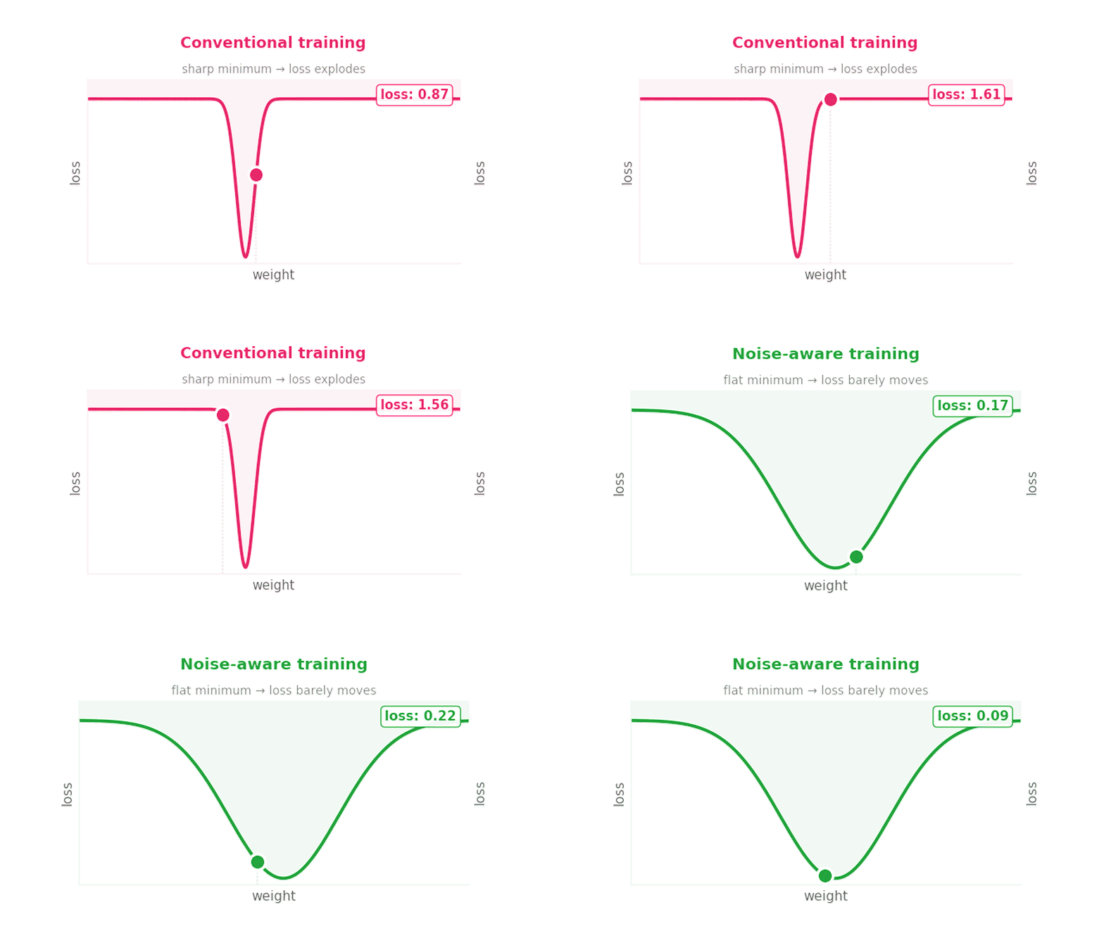
Driving the bit error rate down to the vanishingly small numbers that conventional computing expects is a slow grind of materials science and device engineering, and there are no shortcuts. But AI changes the calculus. If we have access to the models running on the hardware, we don’t necessarily have to chase those punishing reliability targets; we can train the models around the errors instead. Moreover, some models are more resilient to noise than others. Neural networks are remarkably tolerant of noise, which means we can relax the symbol error rate (SER) by a significant margin and let training absorb the imperfection.
That reframes the entire optimization problem. Instead of spending two decades pushing bit error rate (BER) toward zero, we can spend that engineering effort pushing density up, packing more bits per cell, reducing energy consumption, and accepting that the model will learn to live with the occasional mistake.
Revisiting the memory stack
So what does the memory stack actually want to look like for unconventional, dynamical, noisy systems? The workload splits cleanly in two.
First, there’s parameter memory, the weights themselves, which barely change once a model is trained. For an inference accelerator, what we want is something almost permanent and extremely dense; retention is king, and the occasional rewrite is a luxury we don’t need.
Second, there’s working memory, a scratchpad of the transient state, with information that is immediately available but that can fade away and isn’t written back in the model weights.
PCM and RRAM looked like the natural fit for the parameter side, dense and non-volatile, and capable of physically computing weighted sums through Ohm’s and Kirchhoff’s laws. But years spent pushing down their bit error rate left them with area and energy efficiency that simply doesn’t impress next to SRAM-based in-memory computing. Multibit PCM and RRAM for in-memory computing were proposed, mainly in academic publications, but never took off, precisely because of their large noise and variability, which led to larger BER and high error when directly mapping a pre-trained model. And yet, if only we let go of that BER obsession and changed the optimization target, we could pack more bits per cell and program them at lower conductance (less than 1 µS), improving both energy and area efficiency by orders of magnitude.
When it comes to working memory, our wishlist is clear: DRAM-like performance and density, spread across the chip and co-located with the compute. Many small memories next to the logic, not one monolithic block off to the side. The current front-runners to solve this include gain cells, 3D-stacking HBM onto logic dies, and embedded DRAM (eDRAM). We need a high-speed, high-density memory solution that is logic-compatible and ready for scalable manufacturing in the next three to five years. In exchange for that performance, we can afford to sacrifice retention. As long as the speed and density are there, short retention times can simply be managed and optimized at the system architecture level.
The universal memory never showed up, but AI may finally be the workload that tells each technology exactly which job it was born to do.