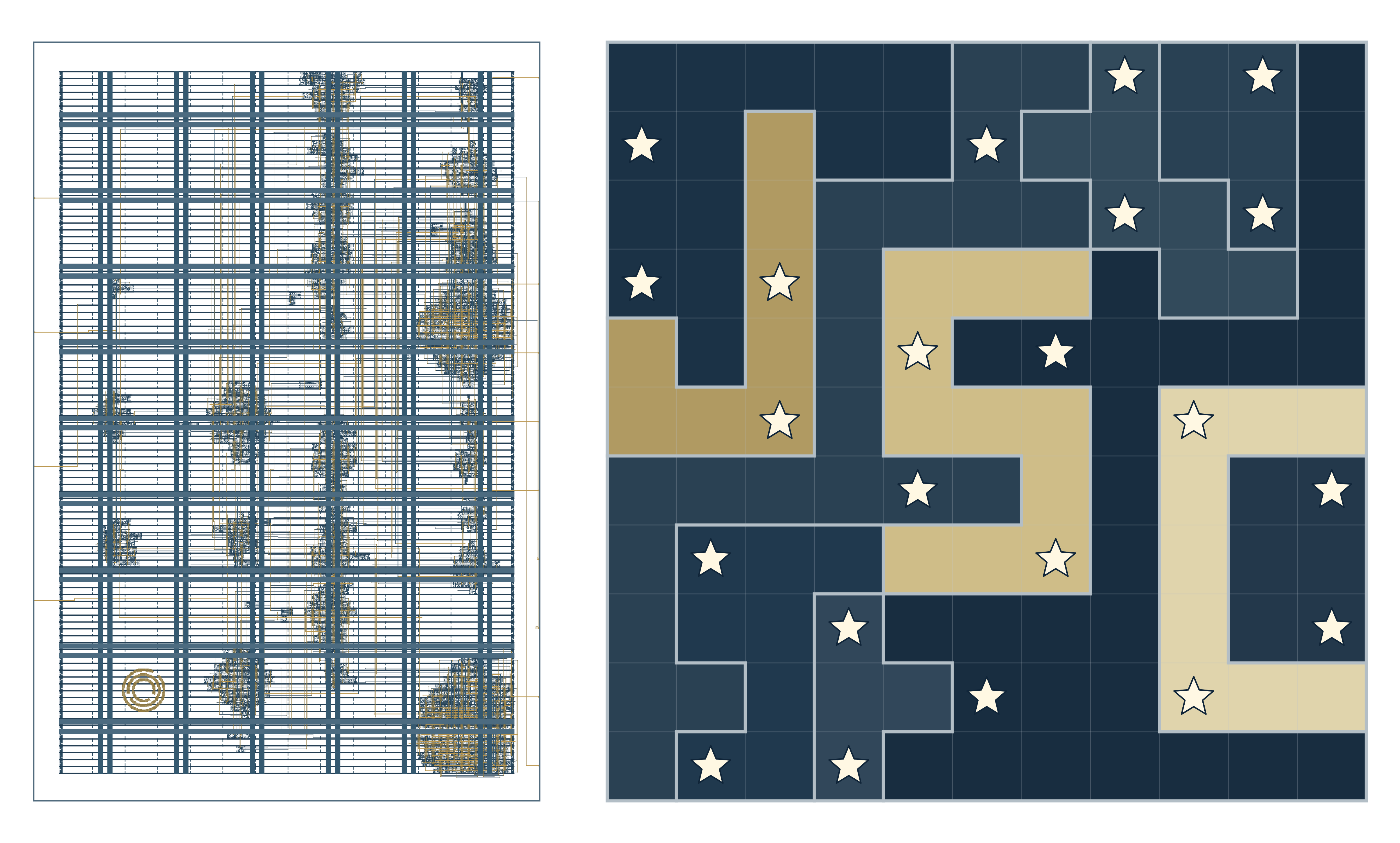
In August, we published a puzzle that handed you the final GDS layout of a small chip and asked you to work out what it did. We supplied the physical layout, but not a netlist or internal signal names, and it was up to you to reverse-engineer the internals.
This post reveals what the chip does and explores the different ways you solved it, with shout-outs to some of our favorite submissions.
The submissions #
We received about 400 submissions from more than 30 countries, the bulk from the US, India, the UK and Australia. Entrants included high school students, researchers, working engineers and retirees. Most solvers used KLayout, Yosys and Z3 alongside custom tools (many AI-written) implemented in Python, Rust, C++, OCaml, Haskell and even Odin.
The solution #
As many of you discovered, the chip is a hardware checker for an 11x11 Star Battle puzzle, also known as “Two Not Touch”. The goal is to place exactly two stars in each row, column, and colored region. No two stars can touch, even diagonally!
The chip accepts 121 cycles of inputs, with each input indicating whether to place a star in the corresponding square. It then runs several parallel checks on these inputs:
A 2-bit counter for each row and every column, requiring that each has exactly 2 stars #
A 121-bit ROM mapping squares to regions, and a 2-bit counter for each region, requiring that each has exactly 2 stars #
A delay line for tracking nearby squares to ensure that two stars never touch, including diagonally. #
A counter for the total number of stars, used to produce certain Easter egg outputs
The puzzle checks are then ANDed together to produce the success signal.
The output generator stores its strings in ROM. To prevent the solution from showing up as plaintext, it is obfuscated with a small LFSR driven based off the game board (though that didn’t stop some of you from attacking the LFSR!)
Once success is achieved, the output logic deobfuscates the solution string and emits it!
(* TWO STARS *)
Most incorrect solutions emit the string “TRY AGAIN”, but a few trigger the Easter eggs listed below.
The puzzle chip was designed using the SKY130 open-source standard cell library, using the LibreLane toolchain.
How you solved it #
Below, we walk through the steps involved in solving the puzzle, with examples from some of our favorite writeups.
Extracting the netlist from the layout
The first step was to extract a gate-level netlist from the GDS layout. To make it a little easier
to get started, we left the cell names (such as sky130_fd_sc_hd__nand2_2) in the GDS files,
allowing the use of the LVS<sup>1</sup> passes in tools like Magic and KLayout to extract a raw gate-level
netlist.
Some folks, however, took on the extra challenge of writing their own netlist extraction tool. Vladislav Shapovalov’s writeup shows how he wrote his own extraction pipeline in C++ to parse the GDS, extract the shapes of each cell, and combine them with the cell names to generate a full logical netlist. He then did a process of trial-and-error with the warm-up design to debug his pipeline before using it to extract the main puzzle GDS.
Simulating the netlist
Recovering the netlist gives you a circuit graph, but simulating it also requires knowing how each cell behaves. Some solvers generated Verilog and used the SKY130 cell models with an existing simulator. Others such as Stephen Ebert, built their own evaluators, computing the logic between registers and updating the registers on each clock edge.
The supplied waveform gave them an input sequence to replay and expected outputs to compare against. The same simulator could then test candidate boards and run the output generator to read the answer.
But matching that waveform didn’t necessarily mean the simulator was correct. Alejandro Soto Franco describes a Python model that reproduced the supplied trace despite getting every tie-high cell wrong. These cells should supply a constant one; the model never evaluated them, leaving their outputs at zero.
The mistake effectively disabled the adjacency check. A solver using that model could therefore find apparently valid boards with touching stars. Alejandro caught the problem by comparing the Python model against a separate Icarus Verilog simulation on additional inputs.
Walking through the logic
A common approach, and the one we most expected, was to start at the “success” output and work backwards through the netlist to identify the conditions for a valid input. We left a few hints in the floorplan: each “island” in the layout corresponded to a single module in the original RTL design.
Sanjay Ravishankar made great use of this, by drawing bounding boxes over each region and then dividing the schematic into these bounding boxes. He includes some great visualizations of this in his writeup. After verifying the module boundaries by looking at connectivity between them, he simulated each module to figure out what it did, and how it fit into the bigger picture.
Dynamic exploration
Another approach was to simulate the chip with different inputs and watch how intermediate signals changed, without worrying too much about the logic functions themselves.
Aaron Shi channeled what he learned in his signals-and-systems class, and “treated the netlist like a system and hit it with impulses at various positions… Then diffed every flop against the all zeros baseline. The flops that change are the response to that one bit,” he writes in his writeup. He then observed that the flops corresponded to the rows, columns, and regions, noting that each of them had to accumulate to exactly 2 to succeed. From this, he constructed a solution grid that met the required conditions for success.
SAT solving
Another approach we saw was to use SAT solvers to find the correct solution without needing to know what the circuit does. In some ways, a SAT solver is perfectly suited to a challenge like this; it can take a circuit encoded over a fixed number of clock cycles and compute the input necessary to make a certain condition evaluate to true (in this case, the success output). Such tools are frequently used in hardware verification as well, by using the SAT solver to prove whether there exists a set of inputs for which a chip will have an undesirable output behavior.
The downside, however, of using a SAT solver for such a challenge is that it doesn’t reveal much about the inner workings of the chip, just the necessary inputs to reach a desired output state. Lokesh Aravapalli, however, found the best of both worlds. He started by using the SAT solver to get a valid set of inputs, but then went back and used these inputs to actually analyze and understand the purpose of the circuit itself, and constructed some cool visualizations of the circuit as well!
Cracking the output generator
With a puzzle like this, there will always be unexpected solutions and unorthodox thinking, as people found ways to solve the puzzle that we didn’t consider while writing it!
One thing that some folks tried was directly extracting the solution string from the output module. The chip included some basic obfuscation in the form of an LFSR<sup>2</sup> to compute a “checksum” of the board, which was then XORed with the solution string before storing it in the ROM (this made it so that simply editing the circuit to drive the “success” input to the output generator would produce a scrambled output). Gabriel Taboada, however, was curious how this all worked, and ended up reverse-engineering the output circuitry to figure out exactly how the solution was encoded and what seed was needed to get the right outputs.
Neat visualizations #
One of our favorite things about reverse-engineering is just how many unique ways there are to approach such a challenge. One of the best ways to see how different people approached the challenge is via the visualizations they built!
Joshua Stapleton built a netlist-layout viewer , that shows both the schematic and the layout side-by-side, showing how the cells connect to each other across hierarchical modules #
José Vargas put together a cool visual walkthrough of how a chip is constructed from PMOS and NMOS transistors and how he extracted them from the layout to figure out the logic function of each cell. #
For anyone who likes solving Star Battle puzzles by hand, Amruth Gulawani made an online playable version of the puzzle encoded in the chip, including some of the special easter-egg outputs on incorrect solutions. #
Possibly our favorite visualization: Kjartan van Driel designed a beautiful interactive animated walkthrough of how a chip is constructed and how all of the functionality in the puzzle chip fits together
Other cool things we saw #
Alexander Smallwood decided to have some extra fun with the puzzle by synthesizing the extracted netlist onto an FPGA , and using the switches and LEDs to represent the I/O of the chip! #
Nikhil Kaniyeri took on the challenge of compiling the netlist into Minecraft command blocks to recreate a playable version of the puzzle in-game . #
David Garner converted the entire chip into an analog SPICE simulation to verify his final solution in the analog domain. #
Marcin Wójcik tried something different: he constructed a Groth16 zero-knowledge proof that could demonstrate that he had the solution without revealing it.
——————————–
The Easter eggs! #
To add some extra fun we added easter eggs to the puzzle, many of which people were able to find! Out of all the submissions, two found all six intended eggs; six people found six of the seven when including the floating-wire bug at the end.
Decoding the two failed attempts in example_inputs.vcd as 7-bit ASCII gives “THE NIGHT SKY
AWAITS” #
The VCD header is dated Sat Dec 31 23:59:60 2016 , a real leap second, and the$version string
nudges you to look at the file in a waveform viewer. #
A row of marks on an otherwise unused layer below the die spells PER ARENAM AD ASTRA in Morse
code: “through the sand, to the stars” #
There are several failure messages. All zeros give EMPTY SKY and all ones giveBIG BANG . A
board that passes the counts but has adjacent stars selects theTWO NOT TOUCH hint;
other rejected inputs getTRY AGAIN . #
About 1,400 isolated squares on met2 form a 57×57 pixel Jane Street logo (you can see it on the image above) #
If you render the eleven regions, their shapes spell out “JSC”. #
The TWO NOT TOUCH output path has an unconnected wire in it, which is why some of you sawTWO"NOT TOUCH in simulation. This one was originally a bug in our layout. We caught it
in an LVS pass but left it as an extra easter egg, to see who would catch it! Plenty of
you diagnosed it down to the floatinga31oi input, and a few helpfully reported it to
us as a bug.
Takeaways #
AI is going to be part of challenges like this, and it is a game changer for building analysis, netlist viewing, and debugging tools. Some entrants described using it for small scripts; others gave agents the whole puzzle. When we first came up with the puzzle we also saw that the latest models could be given a single prompt and, in 30 minutes or less, come up with the final solution. Although this takes away a lot of the fun and learning from working through the puzzle!
Several solvers kept investigating after they had already found the answer. A SAT solver could supply a winning input, but they still wanted to understand what the chip was counting and how its wiring encoded the puzzle’s rules. That curiosity led to some of our favorite writeups: accounts that explained how the circuit worked, rather than stopping when it printed the right string.
Some of the best debugging stories came from solvers deliberately trying to break their own tools. Models that reproduced our sample waveform perfectly still contained mistakes. Comparing separate implementations and constructing inputs that should fail exposed errors that replaying the examples hadn’t caught. That’s a useful habit well beyond puzzles, especially when AI makes it easier to build tools faster than you can check them.
Thanks to everyone who took the time to pull our chip apart, and especially to those who wrote up their process in enough detail for the next person to follow along. There were so many great write-ups that we didn’t get to feature all of them, but we really appreciate the effort everyone made!
If you enjoyed taking our chip apart, try designing your own in our protocol-emulator ASIC competition. The challenge is to build an open-source, programmable chip that can handle protocols like UART, SPI and I2C, with enough flexibility to support new protocols after fabrication. We’ll pay to fabricate our favorite designs, and winners will receive chips and dev boards to test them in real silicon. Submissions close on January 18, 2027.
The hardware team at Jane Street designs FPGAs and ASICs that run some of the fastest trading systems in the world, and the day-to-day work is full of puzzles just like this one: staring at a sea of gates, timing reports, or waveforms and slowly teasing out what’s really going on. These problems are hard in a way that’s deeply satisfying to solve, and honestly, it’s a big part of why we like working here.
If that sounds intriguing, here are some ways of learning more:
Check out our hardware (FPGA and ASIC) internships andfull-time roles. #
Read about Hardcaml (our open-source OCaml hardware design libraries) #
On the academic side, read about our visiting researcher andgraduate fellowship programs.
If you just want to stay in touch, you can fill out this form.
LVS stands for “Layout vs Schematic”, it is usually used at the very end of a chip-design flow to verify that the final layout is logically equivalent to the initial RTL design (e.g., that no wires were dropped or mis-connected during the routing process). However, it can also be used to just extract the netlist from an existing layout file. ↩ 2. Linear Feedback Shift Register, which is a very small circuit that generates a pseudorandom output based on an input bitstream. Often used to compute checksums for data integrity, we used it here to scramble the output string based on a checksum of the solution board. ↩