Kicking off the afternoon presentation blocks for the second day of Hot Chips 2026, the rest of the day is going to be dedicated to server AI accelerators. Once a part of the GPU track, AI accelerators have become the largest track at the show – overtaking CPUs – underscoring just how much in the way of engineering resources have been invested into the chips in order power several projects.
First up on the AI track is meta, who is at the show to present about their custom AI silicon, the Meta Training and Inference Accelerators (MTIA). Earlier this year the company laid out a roadmap for the chips, with plans to release four generations of increasingly complex AI accelerators over the next couple of years. As with the rest of the AI chip vendors presenting today, the emphasis is on producing in-house silicon that is better aligned to the workloads they are expecting, and getting away from buying commodity hardware from the major vendors and paying the margins that entails. Especially as Meta is expecting to need a lot of these chips in order to meet the demand for AI inference in their data centers.
This article is being written live from the presentation, so please excuse any typos.
As of March, Meta’s roadmap calls for releasing four generations of accelerators: the MTIA 300, 400, 450, and 500. MTIA 400 in particular is slated to be a major development for Meta, as it introduces FP4 support, the ability to scale up to a 72 node domain, and a significant increase in overall performance.
Starting things off, Meta is recapping their Deep Learning Recommendation Model (DLRM), and the challenges of training around it. They need to generate millions of recommendations every day. Which can be hard to do with how memory-bound these tasks are.
GPUs are not ideal for DLRM training, in Meta’s eyes. Memory and FLOPS utilization challenges present bottlenecks to training. Not to mention the TCO of operating all of those GPUs. To that end, Meta developed the MTIA, which was their first DLRM training chip.
The 300 was a purpose-fixed silicon chip. The chip is designed to outperform GPUs in this regard. The chip was comprised of 72 processing elements (PEs) and 16 messaging elements (MEs), which were paired up with 216GB of HBM3e memory. The compute die was on 3nm, while the I/O die was on 5nm.
And here’s a look at MTIA 300 performance. It achieves parity with GPUs at a competitive TCO. The high memory and cache bandwidth of the chip, along with purpose-built units, helped them net an over 1.8x speedup in both forward and backwards propagating models.
With Meta’s success on the 300, the company has applied those learnings to the the MTIA 400, which goes back to being an inference chip. The chip is not just for recommendations, but is designed to handle a broader case of inference.
GenAI workloads need immense compute throughput and efficient scaling over many accelerators. Meanwhile the memory capacity needs are greater than ever as the models are getting so large.
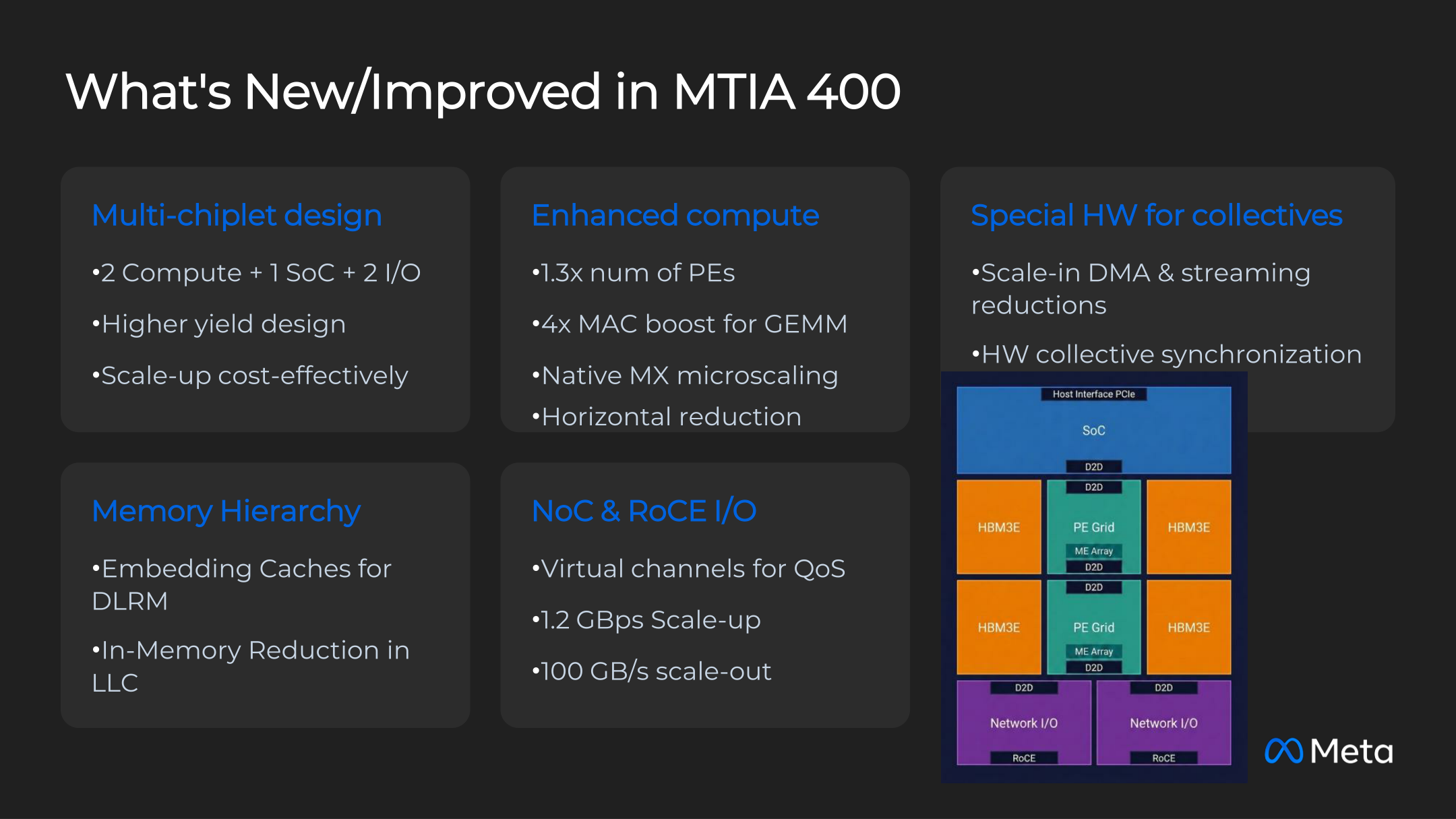
Meta is addressing these goals though some fundamental silicon changes. They are not just using chiplets here, but now an even larger number of chiplet types, with compute, SoC, and I/O chipets. Of course, they have scaled up the amount of computational hardware at the core of this chip. Hardware MXFP4 support is also a big boon in helping Meta push a larger number of FLOPS.
400 also makes some major memory changes. Meta has introduced two types of embedding caches for DLRM.
Taking a look at the 400 package, there are 2 compute chiplets in the middle, which house the core compute engines and collective engines. Along its side are the HBM stacks, while the SoC chiplet is at the top to provide the host connection via PCIe Gen6, and then two networking chiplets sit along the bottom.
Zooming into the compute chiplet and its architecture, Meta is now using an 8×6 grid of PEs for the compute core, and an additional row of PEs for redundancy that are logically drawn along the top. A single processing element contains several fixed function blocks.
Diving a bit further into a PE, here is the dot product to compute registers and the cross-PE reduction. Meta has boosted the MAC array density here, which helps to significantly boost the GEMM performance of the PEs.
For non-GEMM workloads, there is a separate special function unit in the MTIA 400. As with similar chips, it handles things such as non-linear functions and data type conversions. The SFU also has support for a dedicated gather operation, which can grab 64 elements in a single cycle. As mentioned earlier, MTIA adds MXFP4 support. The MX version in particular effectively allows for higher precision via the shared exponent. Meta supports MX4, MS8, and MS8S – a larger 16×16 FP8 block format for training.
Each PE also contains their own CPUs. Two of them, in fact. These CPU-P cores are RISC-V based, and contain both a scalar and vector cores, for general purpose vector operations.
Shifting over to the uncore portion of MTIA 400, here is a look at the chip’s memory hierarchy. There are 8 stacks of HBM3e memory, providing 9.4TB/second of memory bandwidth. This also covers the host embedding cache (HEC), which helps Meta manage the extremely large size of their embedding tables by keeping the hot portions close to the accelerators.
The internal fabric of the 400, or the network-on-chip, as Meta refers to it, is a 2D mesh network. The NoC implements extensive congestion control mechanisms to control things such as leaky buckets. This is also where the ME array is located.
Looking at a single ME, the upgraded MEs in the 400 are their own small processors, complete with their own RISC-V CPU core, which Meta calls their CPU-M. There is also a near memory compute block here, which can move 128 bytes per cycle for DMA operations.
These MEs, in turn, help orchestrate the larger collective flow of the chip. The Ethernet-based scale-up fabric of the chip offers 1.2TB/second of bandwidth, while scale-out networking takes place through the PCIe switch. There is a particular emphasis on eliminating data movement when possible through AllReduce and AllToAll support.
Moving up the hierarchy, a single tray contains four MTIA 400 accelerators. The scale-up fabric allows for 72 ASICs to be placed in a single scale-up domain.
Looking at the performance of a single accelerator chip, the 400 offers 12 PLFOPS of FP4 performance, with smaller amounts at higher precisions. Versus the previous inference accelerator, the MTIA 200, this is over 15x the FP16 compute and a whopping 46x increase in DRAM bandwidth. Not ot mention 5x as much SRAM bandwidth.
MTIA 400’s successors are already in development as well. The 450 offers enhanced GenAI inference performance, while the 500 will focus even more on scaling, matching the broader industry push towards larger scale-up domains going beyond just 72 ASICs in a single domain.